dry etching method

A technology of dry etching and etching rate, which is applied in the direction of semiconductor devices, electrical components, transistors, etc., and can solve other problems such as film damage and the inability to guarantee the quality of dry etching

Inactive Publication Date: 2019-12-31
BOE TECH GRP CO LTD
View PDF4 Cites 0 Cited by
  • Summary
  • Abstract
  • Description
  • Claims
  • Application Information

AI Technical Summary

Problems solved by technology

[0003] When the sensor is integrated with the thin-film transistor substrate, it is necessary to perform a dry etching process on the silicon-containing thin film layer of the silicide material in the thin-film transistor substrate. The damage is also very serious, and the quality of dry engraving cannot be guaranteed

Method used


Image

  • dry etching method
  • dry etching method
  • dry etching method

Examples


Embodiment 1

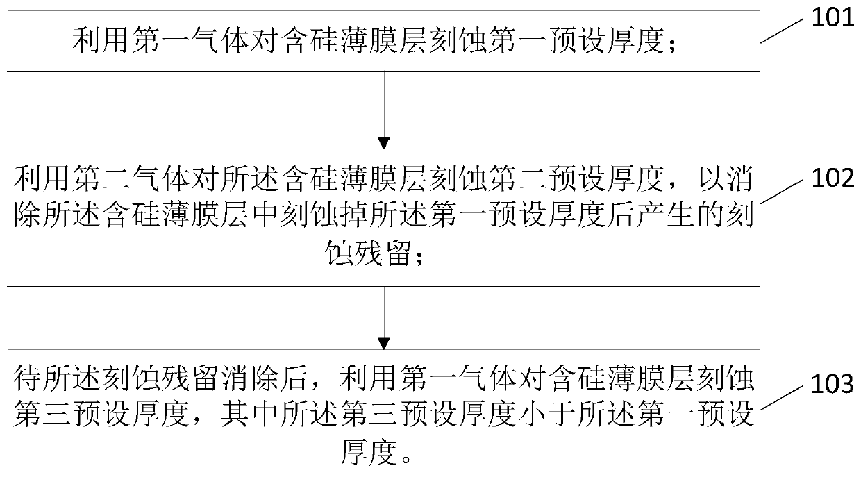
[0047] An embodiment of the present invention provides a dry etching method, including:

[0048] 70% of the thickness of the silicon-containing film layer was etched away by chlorine gas and sulfur hexafluoride gas at a pressure of 45 mTorr, wherein the mass ratio of sulfur hexafluoride gas to chlorine gas was 1:30.

[0049] 20% of the thickness of the silicon-containing thin film layer was etched away by oxygen gas and carbon tetrafluoride gas at a pressure of 45 mTorr, wherein the mass ratio of oxygen gas and carbon tetrafluoride gas was 1:5, and the over-etching amount was 10%.

[0050] 10% of the thickness of the silicon-containing film layer was etched away by chlorine gas and sulfur hexafluoride gas at a pressure of 45 mTorr, wherein the mass ratio of sulfur hexafluoride gas to chlorine gas was 1:30, and the over-etching amount was 20%.

[0051] Wherein, the above-mentioned dry etching temperature is 20 degrees Celsius.

Embodiment 2

[0053] An embodiment of the present invention provides a dry etching method, including:

[0054] 55% of the thickness of the silicon-containing film layer was etched away by chlorine gas and sulfur hexafluoride gas at a pressure of 30 mTorr, wherein the mass ratio of sulfur hexafluoride gas to chlorine gas was 1:30.

[0055] 30% of the thickness of the silicon-containing thin film layer was etched away by using oxygen gas and carbon tetrafluoride gas at a pressure of 30 mTorr, wherein the mass ratio of oxygen gas and carbon tetrafluoride gas was 1:1.5, and the over-etching amount was 20%.

[0056] 15% of the thickness of the silicon-containing thin film layer was etched away by chlorine gas and sulfur hexafluoride gas at a pressure of 30 mTorr, wherein the mass ratio of sulfur hexafluoride gas to chlorine gas was 1:20, and the over-etching amount was 15%.

[0057] Wherein, the above-mentioned dry etching temperature is 30 degrees Celsius.

Embodiment 3

[0059] An embodiment of the present invention provides a dry etching method, including:

[0060] 75% of the thickness of the silicon-containing film layer was etched away by chlorine gas and sulfur hexafluoride gas at a pressure of 30 mTorr, wherein the mass ratio of sulfur hexafluoride gas to chlorine gas was 1:20.

[0061] 15% of the thickness of the silicon-containing thin film layer was etched away by using oxygen gas and carbon tetrafluoride gas at a pressure of 30 mTorr, wherein the mass ratio of oxygen gas and carbon tetrafluoride gas was 1:10, and the over-etching amount was 10%.

[0062] 10% of the thickness of the silicon-containing thin film layer was etched away by chlorine gas and sulfur hexafluoride gas at a pressure of 30 mTorr, wherein the mass ratio of sulfur hexafluoride gas to chlorine gas was 1:20, and the over-etching amount was 15%.

[0063] Wherein, the above-mentioned dry etching temperature is 25 degrees Celsius.


PUM


Abstract

The invention discloses a dry etching method, which relates to the technical field of etching technology. The main purpose is to not only remove etching residues but also reduce damage to other thin film layers during the etching process of silicon-containing thin film layers. Improve etch quality. The main technical solution of the present invention is: a dry etching method, comprising: using a first gas to etch the silicon-containing thin film layer to a first preset thickness; using a second gas to etch the silicon-containing thin film layer to a second predetermined thickness; Set the thickness to eliminate the etching residue generated after etching the first preset thickness in the silicon-containing thin film layer; after the etching residue is eliminated, use the first gas to etch the silicon-containing thin film layer Three preset thicknesses, so that the third preset thickness is smaller than the first preset thickness; wherein, the first gas includes chlorine gas, and the second gas includes fluoride gas. The invention is mainly used for etching the thin film transistor substrate.

Description

technical field [0001] The invention relates to the technical field of etching technology, in particular to a dry etching method. Background technique [0002] In the manufacturing process of the thin film transistor substrate, a dry etching process needs to be adopted. The dry etching process uses plasma generated by a low-pressure gas under a high-frequency electric field to bombard the substrate to perform etching. Specifically, on the one hand, According to the different substrate materials, you can choose the appropriate gas to react with the material to achieve the purpose of etching and removal. On the other hand, you can also use the electric field to guide and accelerate the plasma so that it has a certain kinetic energy. When it bombards When the surface of the substrate is touched, the substances in the substrate will be knocked out, so as to achieve the purpose of physical energy transfer to achieve the purpose of etching. [0003] When the sensor is integrated ...

Claims


Application Information

Patent Timeline
Patent Type & Authority Patents(China)
IPC IPC(8): H01L21/3213
CPCH01L29/6675H01L21/32135H01L21/3213H01L29/786H01L29/66742H01L29/42384
Inventor 刘清召王久石赵磊
Owner BOE TECH GRP CO LTD
Why Eureka
Try Eureka