Two-dimensional crystal material field effect transistor and preparation method thereof

A two-dimensional crystal, field effect transistor technology, applied in semiconductor/solid-state device manufacturing, nanotechnology for materials and surface science, semiconductor devices, etc. Two-dimensional crystal material field effect transistor array and other problems, to achieve the effect of solving unstable performance and simple and feasible production method

Active Publication Date: 2018-01-26
SHANGHAI INTEGRATED CIRCUIT RES & DEV CENT
View PDF8 Cites 10 Cited by
  • Summary
  • Abstract
  • Description
  • Claims
  • Application Information

AI Technical Summary

Problems solved by technology

2) The preparation of two-dimensional crystal material thin films must be on a specific growth substrate, and its process is not compatible with conventional CMOS processes, so it is difficult to prepare small-sized, large-scale two-dimensional crystal material field effect transistor arrays

Method used


Image

  • Two-dimensional crystal material field effect transistor and preparation method thereof
  • Two-dimensional crystal material field effect transistor and preparation method thereof
  • Two-dimensional crystal material field effect transistor and preparation method thereof

Examples


Embodiment Construction

[0030] In order to make the content of the present invention clearer and easier to understand, the content of the present invention will be further described below in conjunction with the accompanying drawings of the specification. Of course, the present invention is not limited to this specific embodiment, and general replacements well known to those skilled in the art are also covered by the protection scope of the present invention.

[0031] Secondly, the present invention uses schematic diagrams for detailed description. When describing the examples of the present invention, for convenience of explanation, the schematic diagrams are not partially enlarged according to the general scale, and should not be used as a limitation to the present invention.

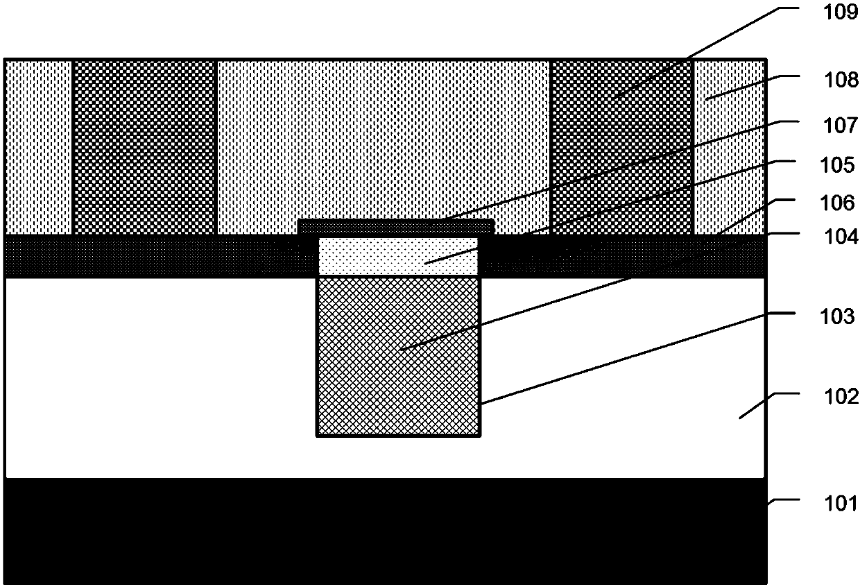
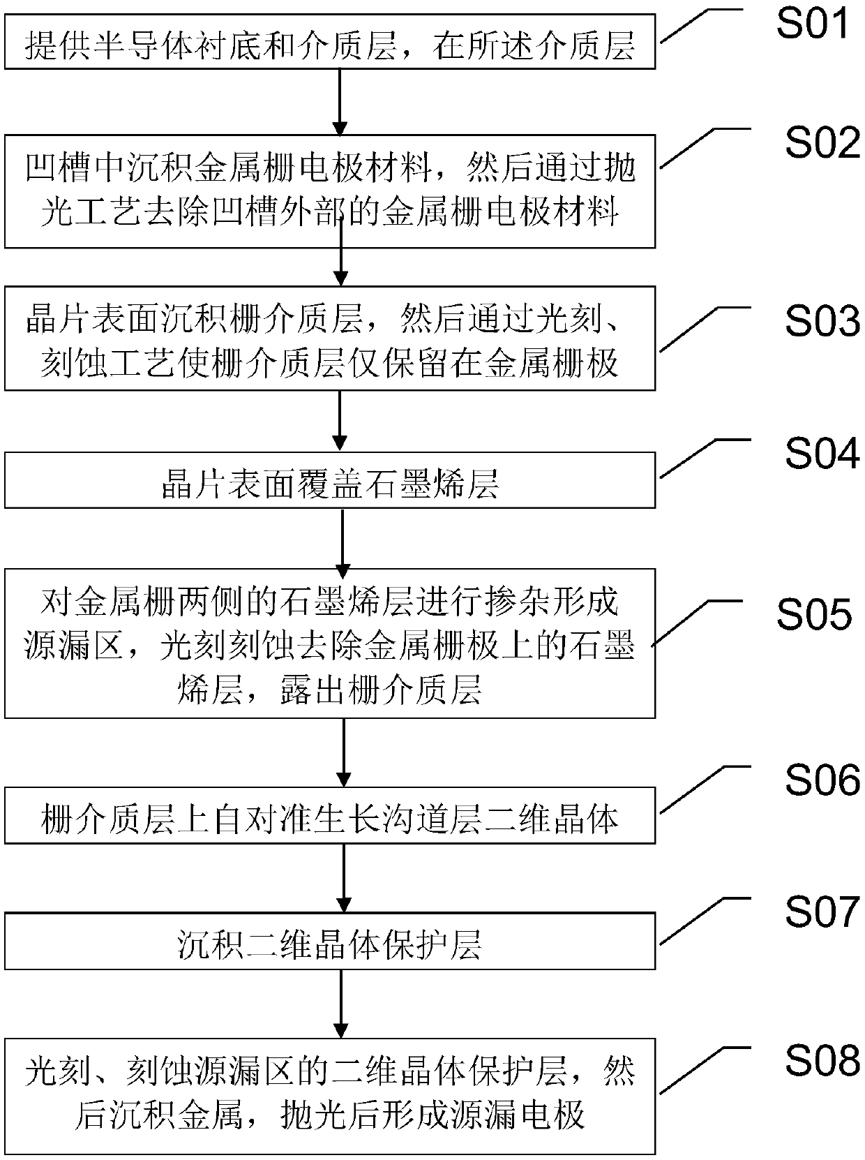
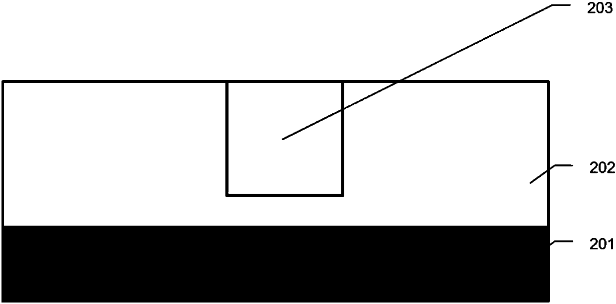
[0032] Now combined with figure 2 The process of the method for preparing the two-dimensional crystal material field effect transistor described in this embodiment is analyzed one by one. The two-dimensional crystalline material...


PUM

PropertyMeasurementUnit
thicknessaaaaaaaaaa
thicknessaaaaaaaaaa
depthaaaaaaaaaa

Abstract

The invention discloses a two-dimensional crystal material field effect transistor, which comprises a semiconductor substrate, a dielectric layer, a metal gate, a gate dielectric layer, a channel layer, a graphene layer, a two-dimensional crystal protection layer, a source electrode and a drain electrode. The invention further discloses a method for preparing the two-dimensional crystal material field effect transistor. A two-dimensional crystal material directly grows on the gate dielectric layer in a self-aligned manner, and doped graphene is adopted as a source and a drain and connected with metal as the source electrode and the drain electrode to prepare the field effect transistor. According to the two-dimensional crystal material field effect transistor and the preparation method thereof, the field effect transistor with stable two-dimensional crystal material film property can be manufactured by adopting a conventional CMOS manufacture procedure; and the ultimate target of preparing a small-size and large-scale two-dimensional crystal field effect transistor array is achieved.

Description

Technical field [0001] The invention belongs to the technical field of semiconductor integrated circuit manufacturing technology, and specifically relates to a two-dimensional crystal material field effect transistor and a preparation method thereof. Background technique [0002] As the feature size of semiconductor devices shrinks proportionally, and chip integration continues to increase, traditional silicon-based semiconductor devices can no longer meet the performance and power requirements of devices and circuits due to process limitations and various negative effects. Major domestic and foreign scientific research institutions and semiconductor manufacturers have studied various new materials and new device structures in order to replace the existing silicon semiconductor devices. Among them, two-dimensional crystal materials can replace silicon channels to prepare semiconductor devices and integrated circuits. In recent years, the technology for preparing transistors from...

Claims


Application Information

Patent Timeline
Patent Type & Authority Applications(China)
IPC IPC(8): H01L29/78H01L29/08H01L29/10H01L29/51H01L21/336B82Y30/00
Inventor 钟旻陈寿面
Owner SHANGHAI INTEGRATED CIRCUIT RES & DEV CENT
Why Eureka
Try Eureka