Graphene transparent antenna and manufacturing method thereof
A technology of graphene and graphene layers, applied in the structural form of radiation elements, etc., can solve problems such as poor conductivity and poor transmittance of transparent antennas, and achieve the effects of solving conductivity problems, ensuring transmittance, and improving radiation efficiency
- Summary
- Abstract
- Description
- Claims
- Application Information
AI Technical Summary
Problems solved by technology
Method used
Image
Examples
Embodiment 1
[0045] In this embodiment, the material of the transparent base material 1 is a quartz plate, put the quartz plate substrate into isopropanol, clean it ultrasonically for 30 minutes, then take out the quartz plate substrate, dry it with nitrogen gas with a purity of 99.999%, and put it into a vacuum Heat it in an oven to 80° C., and bake for 30 minutes; a layer of 5 nm ultra-thin copper metal is plated on the upper surface of the quartz substrate by electron beam evaporation, which is the ultra-thin metal layer 2 .
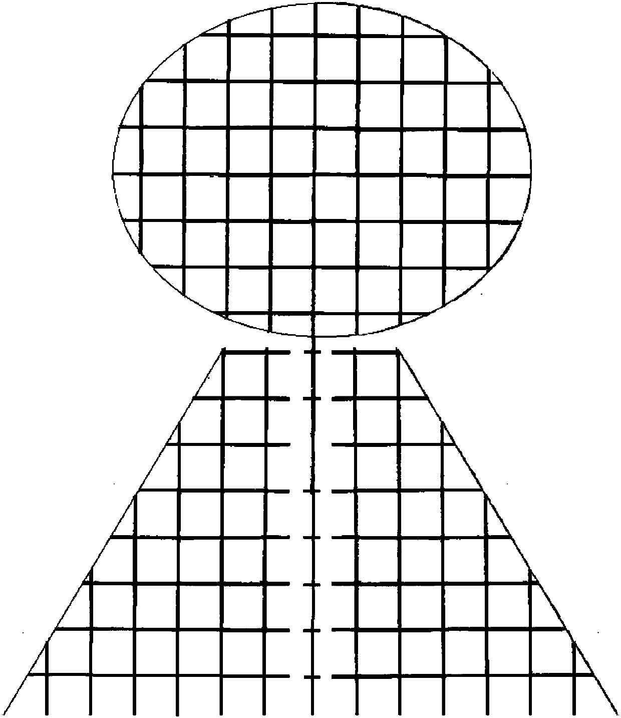
[0046] Make an antenna shape with an elliptical face antenna and its feeder structure (such as figure 1 ) mask plate structure, and use photolithography technology to make the ultra-thin metal layer into an ultra-thin metal layer 2 with a predetermined antenna shape.
[0047] The specific photolithography steps are as follows:
[0048] (1) Coating: spin-coat photoresist on the ultra-thin copper metal layer / quartz sheet, the speed is 3000rad / s, the acceleration is...
Embodiment 2
[0060] Put the quartz substrate into isopropanol, ultrasonically clean it for 30 minutes, then take out the quartz substrate, dry it with nitrogen with a purity of 99.999%, put it in a vacuum oven, heat it to 80°C, and bake it for 30 minutes; The upper surface of the substrate is plated with a layer of 5nm ultra-thin copper metal by electron beam evaporation.
[0061] Fabricate the mask structure (e.g. figure 2 As shown), the macroscopic structure of the mask plate is an elliptical surface antenna and its feeder shape, the internal structure of the antenna is a grid shape, the grid period is 500 μm, the line width is 4 nm, the duty cycle is 10%, and the thickness is 5 nm.
[0062] Then, using the same photolithography method as in Embodiment 1, the ultra-thin metal layer is fabricated into an ultra-thin metal grid layer with a predetermined antenna shape.
[0063] Secondly, put the antenna-shaped copper metal grid layer / quartz sheet into the cavity of the CVD furnace, pass i...
Embodiment 3
[0066] Put the quartz substrate into isopropanol, ultrasonically clean it for 30 minutes, then take out the quartz substrate, dry it with nitrogen with a purity of 99.999%, put it in a vacuum oven, heat it to 80°C, and bake it for 30 minutes; The upper surface of the substrate is plated with a layer of 5nm ultra-thin copper metal by electron beam evaporation.
[0067] Fabricate the mask structure (e.g. figure 2 As shown), the macroscopic structure of the mask plate is an elliptical surface antenna and its feeder shape, the internal structure of the antenna is a grid shape, the grid period is 500um, the line width is 4nm, the duty cycle is 10%, and the thickness is 5nm.
[0068] Then, using the same photolithography method as in Embodiment 1, the ultra-thin metal layer is fabricated into an ultra-thin metal grid layer with a predetermined antenna shape. Subsequently, put the antenna-shaped copper metal grid layer / quartz sheet into the cavity of the CVD furnace, pass in argon ...
PUM
| Property | Measurement | Unit |
|---|---|---|
| Thickness | aaaaa | aaaaa |
| Thickness | aaaaa | aaaaa |
| Sheet resistance | aaaaa | aaaaa |
Abstract
Description
Claims
Application Information


