[0028] The additive manufacturing device and method involved in the present invention will be described in detail below with reference to the accompanying drawings.
[0029]
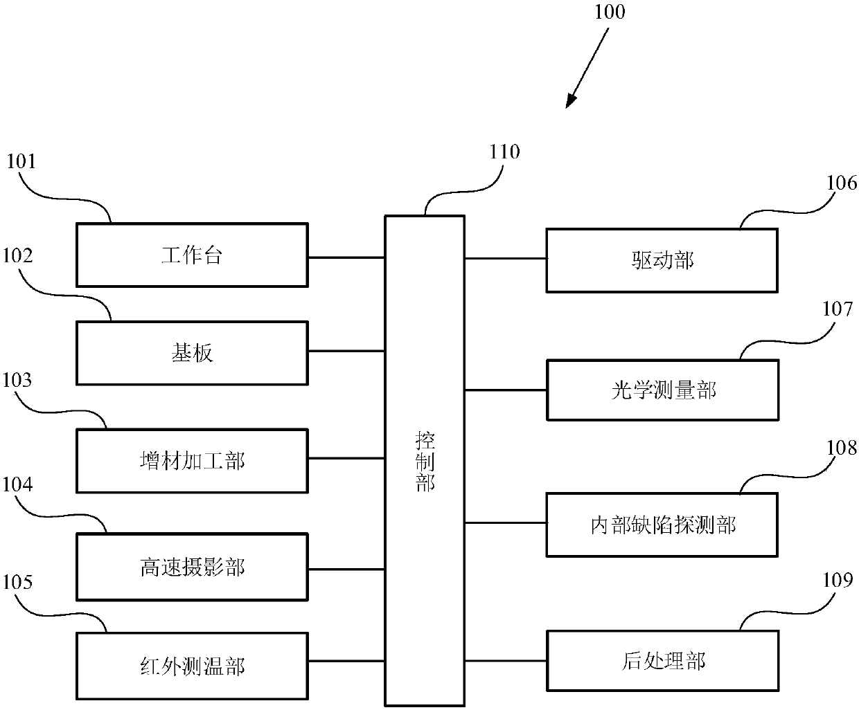
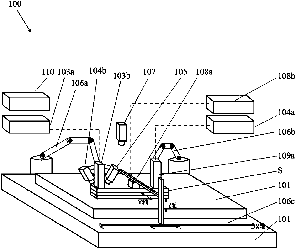
[0030] Such as figure 1 As shown, the additive manufacturing apparatus 100 includes: a workbench 101, a substrate 102, an additive processing unit 103, a high-speed photography unit 104, an infrared temperature measurement unit 105, a drive unit 106, an optical measurement unit 107, an internal defect detection unit 108, and a rear The processing unit 109 and the control unit 110.
[0031] Such as figure 2 As shown, the substrate 102 is placed on the workbench 101 to carry the material to be processed, has a heating function, preheats the processing environment, and suppresses stress concentration.
[0032] The additive processing unit 103 includes a high-energy beam generator 103a and an additive processing head 103b. The high-energy beam generator 103a can generate a high-energy beam and transmit it to the additive processing head 103b; the additive processing head 103b moves according to the set motion path, melts the material to be processed during the movement, and sinters to form a deposited layer of the required shape and size S. Here, the high-energy beam generator 103a can be a laser, an electron beam generator, an arc power source, or a plasma arc power source; correspondingly, the additive processing head 103b corresponds to a laser optical processing head, an electromagnetic lens, an arc welding gun, and a plasma arc welding gun. In this embodiment, the additive processing head 103b also includes a device for filling materials, such as a wire filling device or a powder feeding device.
[0033] The high-speed camera 104 is used to detect the shape of the molten pool, and it includes a camera 104a and an image processing transmitter. The camera 104a and the additive processing head 103b move synchronously to capture images of the material processing and molding conditions; the image processing transmitter processes the captured data and transmits the processed material image information to the control unit 110.
[0034] The infrared temperature measuring part 105 is used to detect the temperature of the molten pool, and it includes a temperature measuring head 105a and a processing transmitter. The temperature measuring head 105a and the additive processing head 103b move synchronously to detect the temperature distribution of the material; the temperature processing transmitter processes the detected data and transmits the processed material temperature distribution information to the control unit 110.
[0035] The driving unit 106 includes a first robot arm 106a, a second robot arm 106b, and a three-dimensional motion mechanism 106c. The first mechanical arm 106a and the second mechanical arm 106b are both installed on the side of the workbench 101, and their front ends can move freely and cover the entire workbench 101. The three-dimensional motion mechanism 106c is installed on the side of the workbench 101, and the moving end can cover the entire workbench 101 for free movement.
[0036] The front end of the first mechanical arm 106a is used to install the additive processing head 103b, the camera 104a and the temperature measuring head 105a, and to drive the additive processing head 103b, the camera 104a and the temperature measuring head 105a to move synchronously.
[0037] The optical measuring part 107 is fixedly installed above the substrate 102 and facing the deposition layer S, and is used for detecting material surface defects and forming dimensions, and obtaining inspection information.
[0038] The internal defect detection unit 108 is used to detect internal defects of the material, and it includes a detection head 108a, a detection generator 108b, and a detection analysis transmitter. The detection head 108a is close to the deposition layer S for surface scanning; the detection generator 108b transmits energy to the detection head 108a; the detection analysis transmitter analyzes and determines the type and location of the defect inside the deposition layer S according to the scanning situation of the detection head 108a, and determines the defect type And the location information is sent to the control unit 110. Here, the probe 108a is an ultrasonic or X-ray probe 8, and correspondingly, the probe generator 108b is an ultrasonic or X-ray generator.
[0039] The moving end of the three-dimensional motion mechanism 106c is used to install the probe 108a and drive the probe 108a to move;
[0040] The post-processing part 109 is used for processing the material defect area in a corresponding post-processing manner, and includes a post-processing processing head 109a and a post-processing device. The post-processing head 109a can move to be close to the upper surface of the material defect area, and gradually post-process the material defect area to eliminate the defects. In this embodiment, the post-processing head 109a includes: a mechanical roller, a laser impact head, and a stirring head There are three processing heads. One of the processing heads is selected according to the processing method during each processing; the post-processing device is used to provide energy to the post-processing processing head 109a, which includes the power supply, pulse laser, and mechanical device; here, the post-processing method It includes at least one post-processing method among mechanical rolling processing, laser shock strengthening processing, and friction stir processing processing, and can be automatically switched.
[0041] The front end of the second mechanical arm 106b is used to install the post-processing head 109a and drive the post-processing head 109a to move;
[0042] The control unit 110 communicates with the additive processing unit 103, the high-speed photography unit 104, the infrared temperature measurement unit 105, the first robotic arm 106a, the optical measurement unit 107, and the internal defect detection unit 108 to control their operation and obtain Material image information, material temperature distribution information, inspection information, defect type and location information, and determine whether there are defects and whether the defects can be eliminated based on these information. If there are defects that can be eliminated, determine the defect processing area, each The post-processing path and post-processing method corresponding to the area, control the post-processing part 109 to follow the corresponding post-processing path, and adopt the corresponding post-processing method to process each defect processing area separately; in the case of irreversible defects Stop processing and alarm. In this embodiment, the control unit 110 is a computer, which can also display processing status information in real time, and allow the operator to input or select corresponding information, that is, the control unit 110 can set the process parameters and parameters of the equipment controlled by it. Its workflow.
[0043] Based on the above structure, the method of using the additive manufacturing device 100 for additive manufacturing is:
[0044] (1) The high-energy beam generator 103a generates a high-energy beam and transmits the energy to the additive processing head 103b. The additive processing head 103b melts the material to form a molten pool. Driven by the first robotic arm 106a, the additive processing head 103b Moving according to the set movement path, the deposition layer S is gradually formed, and different shapes of the deposition layer S are obtained according to the different movement paths;
[0045] (2) During the sintering process, the first mechanical arm 106a drives the camera 104a and the temperature measuring head 105a to move the molten pool synchronously with the additive processing head 103b, and takes image shots of the material processing and shaping conditions to obtain material image information. , To detect the temperature distribution of the material to obtain material temperature distribution information, which is fed back to the control unit 110 by the image processing transmitter and the temperature processing transmitter;
[0046] (3) After sintering one or more layers, the additive processing head 103b, the camera 104a and the temperature measuring head 105a stop working, and move out of the sintering work area with the first mechanical arm 106a;
[0047] (4) The optical measurement unit 107 detects surface defects and forming dimensions, and feeds back the detected material temperature distribution information to the control unit 110;
[0048] (5) The internal defect detection unit 108 starts to work. The detection head 108a is driven by the three-dimensional movement mechanism 106c to scan the deposition layer S. The detection analyzer analyzes the scanning situation to determine the type and position of the defect inside the deposition layer S, and This information is fed back to the control unit 110;
[0049] (6) After the detection is completed, the detection head 108a stops working and moves out of the sintering work area with the three-dimensional motion mechanism 106c;
[0050] (7) The control unit 110 comprehensively analyzes the defect form and specific location of the deposited layer S, and judges whether it can be eliminated according to the size and quantity of the defect. If it can be eliminated, determine the defect location, plan the scanning path (post-processing path), scanning range (defect processing area), post-processing method and process parameters of the post-processing processing head 109a, so as to execute the post-processing process. If it cannot be eliminated, stop processing and alarm. If there are no defects, the next layer is sintered. If it is a pore type defect, when its size exceeds the effective working size of the post-processing head 109a, it is judged that the size cannot be eliminated, and the processing is stopped and an alarm; if it is a small-size pore or crack and other defects, the next post-processing processing is performed process;
[0051] (8) The control unit 110 determines the optimal post-processing scan path and scan range: such as image 3 As shown, when the material defects are multiple defects or single defects distributed in local clusters, the diameter d of the smallest circle that contains all the defects in the local area is used to represent the characteristic size of the defect area, and the scan area position is the area contained in the circle, and the scan path To circle the spiral line with the largest diameter d in this area, the scanning start position is the center point of the spiral line; Figure 4 As shown, the chain-like distribution of multiple defects, the length l and width w of the strip area covering all the defects in the local area represent the characteristic size of the defect area, the scanning area position is the strip area, and the scanning path is this strip The scanning start position is one of the end points of the strip-shaped area.
[0052] (9) The control unit 110 determines the optimal post-processing mode and process parameters according to the following categories:
[0053] ●Mechanical rolling technology: suitable for all metals, and also suitable for large and medium-sized deposition layers S, such as deposition layers S with a width greater than 2mm. Working process: mechanical rollers exert mechanical force on the deposition surface to make the surface smooth and compact Internal pore defects; the selection of parameters is as follows: 1) The traveling speed range of the processing head is 0.5-5m/min; 2) The lower pressure of the processing head: depends on the type of material, generally should be greater than the yield strength of the material;
[0054] ●Laser shock strengthening treatment technology: high-strength materials such as titanium alloy, high-temperature alloy, high-strength steel, the width of the deposition layer S is less than 0.5mm; working process: the constrained layer of the laser shock head covers the flat deposition layer S, the pulse laser works, the laser beam is transparent The over confinement layer generates a plasma shock wave, impacts the deposition layer S, causes plastic deformation of the material, eliminates pore defects and stress concentration in the deposition layer S, and strengthens the deposition layer S material; the process parameters are as follows: 1) The processing head travel speed range is 0.5 ~5m/min; 2) Laser energy parameters: 0.5~5GW/cm 2;
[0055] ●Surface friction stir processing technology: low-strength non-ferrous metal materials such as aluminum alloy, magnesium alloy, copper alloy, etc., and also suitable for thick-walled structures, such as the width of the deposited layer S is greater than 5mm, and the surface is flat. The parameters are as follows: 1) Stirring head speed : Aluminum alloy/magnesium alloy 1500-2000 revolutions, copper alloy 2000-3000 revolutions; 2) Stirring depth: It depends entirely on the depth of the deposition layer S, the depth of the deposition layer S is as much as the stirring depth, which is generally less than 5mm in this technology; 3) The walking speed of the processing head: depends on the depth of the deposited layer S and the type of material. Generally speaking, when the thickness of the deposited layer S is less than 5mm, the maximum of aluminum alloy magnesium alloy can reach 0.8m/min, and the maximum of copper alloy can reach 0.5m/min ;
[0056] ●Composite post-processing method:
[0057] a) Mechanical rolling + laser shock strengthening method: titanium alloy, high-strength steel, high-temperature alloy, mechanical rolling can not eliminate all defects of the deposition layer S, the surface flatness error of the deposition layer S is greater than 1mm, the processing process is first mechanical rolling, Then laser shock;
[0058] b) Mechanical rolling + surface friction stir treatment method: aluminum alloy, magnesium alloy, copper alloy, mechanical rolling cannot eliminate all defects of the deposition layer S, the surface flatness error of the deposition layer S is greater than 1mm; the processing process is mechanical rolling first , And then surface friction stir treatment;
[0059] (10) The specific process of the post-treatment process is: the post-treatment processing head 109a is driven by the second mechanical arm 106b to move close to the upper surface of the deposition layer S, and the post-treatment processing head 109a gradually follows the scheme determined in (8) and (9). Scan the impact deposition layer S and perform post-processing until all the surfaces of the defect area of the deposition layer S are processed, and then the post-processing processing head 109a is reset with the second mechanical arm 106b;
[0060] (11) The additive processing head 103b moves above the deposition layer S to start the processing of the next deposition layer S, and the above process is repeated until the processing is completed.
[0061] The above description is only illustrative but not restrictive to the present invention. Those of ordinary skill in the art understand that changes and modifications can be made based on the above disclosure without departing from the spirit and scope defined by the claims. Or equivalent, but all fall within the protection scope of the present invention.
[0062] As above, this solution introduces online non-destructive testing technology and selective post-processing methods into the additive manufacturing process, through organic combination to form a new type of additive manufacturing method and equipment, which effectively solves the defects of additive manufacturing and material performance problems, and has better performance. The short processing time can break through the bottleneck of metal additive manufacturing technology and realize high-quality and efficient additive manufacturing.
[0063] The above embodiments are merely illustrative of the technical solutions of the present invention. The additive manufacturing apparatus and method involved in the present invention are not only limited to the structures described in the above embodiments, but are subject to the scope defined by the claims. Any modification or supplement or equivalent replacement made by a person skilled in the art to which the present invention belongs on the basis of this embodiment is within the scope of protection claimed by the present invention.