Misreading-resistant resistive random access memory and preparation method thereof

A resistive variable memory and resistive variable technology, applied in the direction of electrical components, etc., can solve the problems of poor uniformity and stability, scattered switching voltage, high power consumption, etc., achieve good stability and uniformity, improve uniformity, and low power consumption Effect

Active Publication Date: 2018-02-09
上海夯业真空设备科技有限公司
View PDF7 Cites 5 Cited by
  • Summary
  • Abstract
  • Description
  • Claims
  • Application Information

AI Technical Summary

Problems solved by technology

[0004] The purpose of the present invention is to provide a resistive variable memory that avoids misreading and its preparation method, so as to solve the problems of excessive dispersion of switching voltage, poor uniformity and stability, and high power consumption in the existing resistive variable memory

Method used


Image

  • Misreading-resistant resistive random access memory and preparation method thereof
  • Misreading-resistant resistive random access memory and preparation method thereof
  • Misreading-resistant resistive random access memory and preparation method thereof

Examples


Embodiment 1

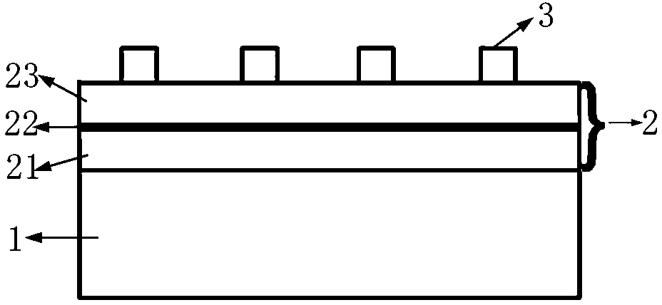
[0032] like figure 1 As mentioned above, the resistive memory provided by the present invention to avoid misreading, its structure includes Pt / Ti / SiO sequentially from bottom to top 2 / Si substrate 1, in Pt / Ti / SiO 2 The resistive medium layer 2 formed on the Pt film layer of the Si substrate 1 and the Ag electrode layer 3 formed on the resistive medium layer 2 . The resistive dielectric layer 2 sequentially includes a first zirconium hafnium oxide film layer 21 , a graphene oxide quantum dot intermediate layer 22 and a second zirconium hafnium oxide film layer 23 from bottom to top.

[0033] The thickness of the resistive medium layer 2 is 10-20 nm, wherein the thickness of the graphene oxide quantum dot intermediate layer 22 is 0.8-1.2 nm, preferably 1 nm; the first zirconium hafnium oxide film layer 21 and the second zirconium hafnium oxide film The thickness of the layers 23 is preferably the same.

[0034] The thickness of the Ag electrode layer is 50-200 nm.

[0035] ...

Embodiment 2

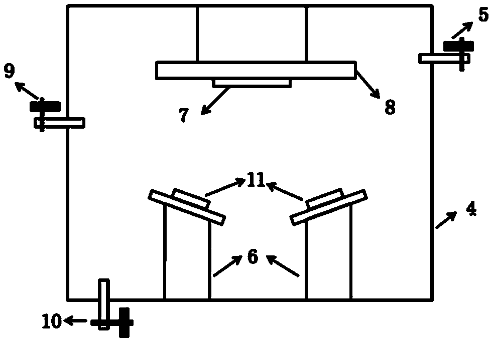
[0045] (1) Pt / Ti / SiO 2 / Si substrate 1 is placed in a beaker filled with acetone, cleaned with ultrasonic waves for 10 minutes, then placed in a beaker filled with alcohol and cleaned with ultrasonic waves for 10 minutes, then taken out with a clip and placed in a beaker filled with deionized water and cleaned with ultrasonic waves 5min, then take out, nitrogen (N 2 ) to dry.

[0046] (2) Open the chamber 4 of the magnetron sputtering equipment, take out the tableting table 7, first polish it with sandpaper until it shines, clean the organic matter attached to the surface of the tableting table with acetone, and finally wipe it with alcohol; Pt / Ti / SiO 2 / Si substrate 1 is placed on the tableting table 7 for tableting, and Pt / Ti / SiO is guaranteed during tableting 2 / Si substrate 1 is firmly pressed on the table 7 and flattened to ensure uniform growth of the film during sputtering. After the tabletting is completed, it is placed on the substrate table 8 in the chamber 4, and...

Embodiment 3

[0056] Example 3 Testing the performance of the resistive memory prepared by the present invention and the comparative example

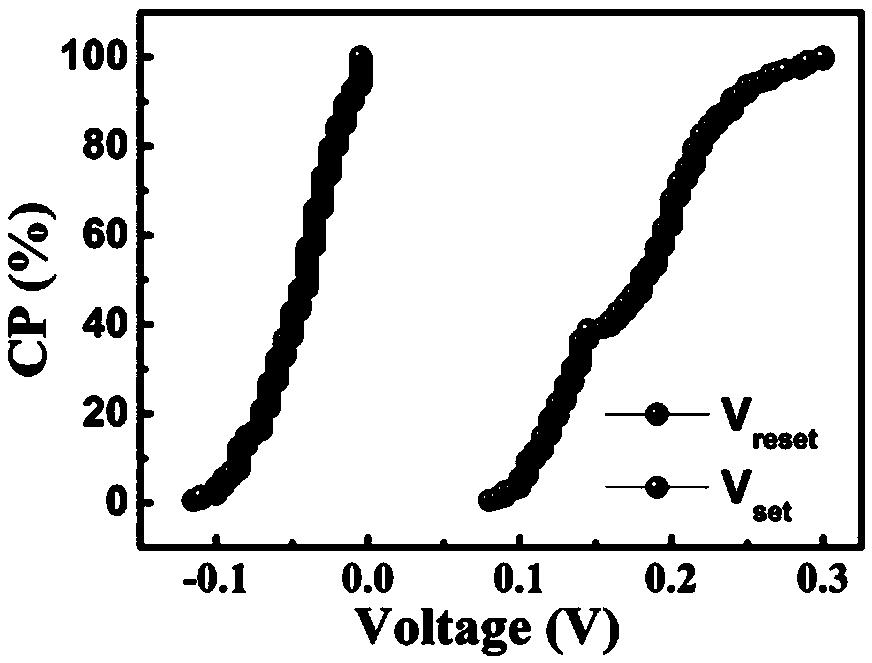
[0057] (1) 200 cycles of current and voltage scans were performed on the resistive memory prepared in Example 2 of the present invention and the resistive memory prepared in Comparative Example 1, and the cumulative probability distribution of the on-off and off voltages was counted. The results are as follows: image 3 (the present invention) and Figure 4 (Comparative Example 1), from image 3 It can be seen that the turn-on voltage of the device, that is, the set voltage, is distributed between 0.08V and 0.3V, and most of them are mainly distributed between 0.15V and 0.2V. image 3 It can be seen that the off voltage, that is, the reset voltage, is distributed between -0.14V~-0.01V, and most of them are mainly distributed between -0.05V~-0.1V. from Figure 4 It can be seen that the turn-on voltage of the device is distributed between 0.08V and ...


PUM

PropertyMeasurementUnit
thicknessaaaaaaaaaa
thicknessaaaaaaaaaa
thicknessaaaaaaaaaa

Abstract

The invention discloses a misreading-resistant resistive random access memory. The structure of the misreading-resistant resistive random access memory comprises a substrate, a resistive random dielectric layer which is formed on the substrate and an Ag electrode layer which is formed on the resistive random dielectric layer, wherein the substrate, the resistive random dielectric layer and the Agelectrode layer are arranged from the bottom to the top in turn. The resistive random dielectric layer comprises a first zirconium hafnium oxide film layer, a graphene oxide quantum dot intermediate layer and a second zirconium hafnium oxide film layer which are arranged from the bottom to the top in turn. The invention also discloses a preparation method of the resistive random access memory. Theresistive random access memory of the specific structure is prepared, especially graphene oxide quantum dot intermediate layer is embedded between the first zirconium hafnium oxide film layer and thesecond zirconium hafnium oxide film layer of the resistive random material layer and growth and fracture of the conductive filament can be accurately controlled to enhance the uniformity of the device so that the finally prepared resistive random access memory is enabled to have the more stable resistance change, lower power consumption and better stability and uniformity, and the preparation method is simple, great in operability and simple in large-scale production and manufacturing and thus the application prospect is wide.

Description

technical field [0001] The invention relates to a memory and a preparation method thereof, in particular to a resistive memory and a preparation method for avoiding misreading. Background technique [0002] In recent years, Nanoscale Resistive Switching Radom Access Memory (RRAM) has become one of the potential candidates for next-generation high-density memory due to its simple structure, fast access speed, low power consumption and easy integration. , and has been extensively studied. [0003] The resistive memory is a typical sandwich structure based on the top electrode-dielectric layer-bottom electrode. It mainly utilizes the reversible transition between high and low resistance states in the intermediate dielectric layer under the action of different electrical excitations to store data. However, many problems need to be overcome to put the resistive memory into large-scale practical applications. One of the key problems is that the open and close voltages (i.e., set...

Claims


Application Information

Patent Timeline
Patent Type & Authority Applications(China)
IPC IPC(8): H01L45/00
CPCH10N70/24H10N70/011H10N70/8833
Inventor 闫小兵张磊王静娟李小燕
Owner 上海夯业真空设备科技有限公司
Why Eureka
Try Eureka