Method of increasing high-aspect ratio photoetching process windows through dual graph technology

A high aspect ratio, dual pattern technology, applied in electrical components, semiconductor/solid-state device manufacturing, circuits, etc., can solve the problems of insufficient process window lithography process window, insufficient lithography process window, abnormal production line, etc., to increase the process Effects of window, line width reduction, pixel size reduction

Inactive Publication Date: 2018-02-23
SHANGHAI HUALI MICROELECTRONICS CORP
View PDF5 Cites 3 Cited by
  • Summary
  • Abstract
  • Description
  • Claims
  • Application Information

AI Technical Summary

Problems solved by technology

[0003] At present, the hierarchical graphic structure of existing products is a 2D DOT graphic, and the space between repeated DOTs is the key graphic of the pixel area. With the current photoresist thickness, the aspect ratio is greater than 10:1. Thickness, with the exposure method of 2 exposures, the process window of lithography has reached the limit and occasionally there will be abnormalities in the production line caused by insufficient lithography process window
According to the customer's process development requirements for this level, when the pixel size continues to decrease, the pattern structure of DOT is more likely to cause pattern collapse, that is, the photolithography process window is insufficient

Method used


Image

  • Method of increasing high-aspect ratio photoetching process windows through dual graph technology
  • Method of increasing high-aspect ratio photoetching process windows through dual graph technology
  • Method of increasing high-aspect ratio photoetching process windows through dual graph technology

Examples


Embodiment Construction

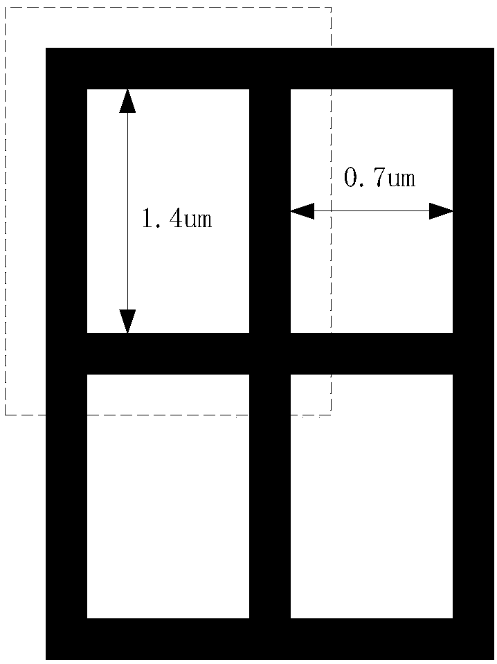
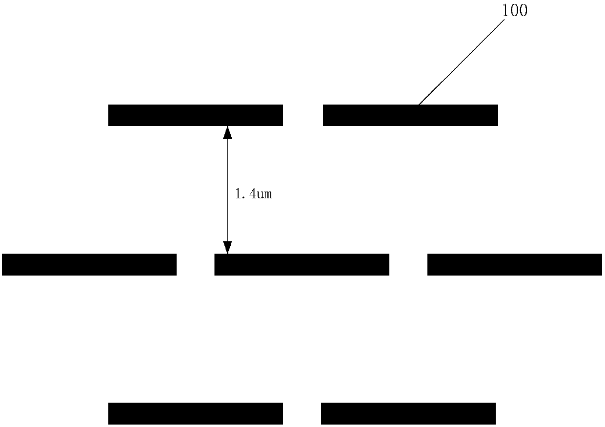
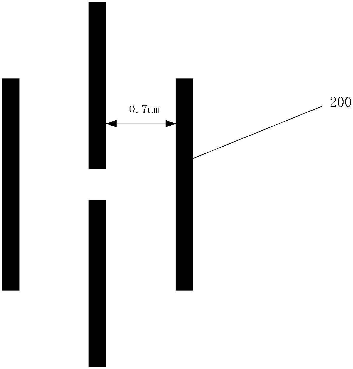
[0021] The specific embodiments of the present invention are given below in conjunction with the accompanying drawings, but the present invention is not limited to the following embodiments. Advantages and features of the present invention will be apparent from the following description and claims. It should be noted that all the drawings are in very simplified form and use imprecise ratios, which are only used for the purpose of conveniently and clearly assisting in describing the embodiments of the present invention.

[0022] The present invention proposes a method for increasing the process window of high aspect ratio photolithography through double patterning technology, comprising the following steps:

[0023] Divide the process requirements of lithography into a combination of two lithography;

[0024] Using the first photomask to perform the first photolithography process on the process pattern;

[0025] Using the second photomask to perform a second photolithography ...


PUM


Abstract

The invention provides a method of increasing high-aspect ratio photoetching process windows through a dual graph technology. The method comprises the following steps: photoetching process requirements are divided to a combination of twice photoetching; a first photomask is used to carry out first photoetching processing on a process graph; a second photomask is used to carry out second photoetching processing on the process graph, and wherein the process window graph formed by the combination of the first photomask and the second photomask has a pixel size meeting the process requirements andare 1D groove graph photomasks. According to the method of increasing the high-aspect ratio photoetching process windows through the dual graph technology, in view of the high-aspect ratio layer, when the pixel size is reduced gradually and a target linewidth is reduced, the dual graph technology is adopted to split a one-layer 2D point graph to a two-layer 1D groove graph, and in combination ofthe PSM photomask process mode, the high-aspect ratio layer process windows are increased.

Description

technical field [0001] The invention relates to the field of semiconductor integrated circuit manufacturing, and in particular to a method for increasing a high-aspect-ratio photolithography process window through a double patterning technique. Background technique [0002] At present, there is a photoresist layer with an aspect ratio exceeding 10:1 in the process. The purpose of this layer is to isolate the pixel area. When the ion implantation dose in the pixel area is larger, the function of the device will be stronger; at the same time, this layer is also along the The representative level of the development of "Moore's Law", the three main directions promoted by the industry: the reduction of pixel size, the reduction of key dimensions, and the thickening of photoresist. [0003] At present, the hierarchical graphic structure of existing products is a 2D DOT graphic, and the space between repeated DOTs is the key graphic of the pixel area. With the current photoresist t...

Claims


Application Information

Patent Timeline
Patent Type & Authority Applications(China)
IPC IPC(8): H01L21/027
CPCH01L21/0274
Inventor 张涛王晓龙李德建吴鹏
Owner SHANGHAI HUALI MICROELECTRONICS CORP
Why Eureka
Try Eureka