
8-shaped inductor structure integrated on semiconductor chip, and semiconductor structure

A semiconductor, figure-8 technology, applied in the field of microelectronics, can solve the problems of low substrate resistivity and difficulty in integrating inductance, and achieve the effect of enhancing stability and reliability, small parasitic capacitance, and exerting performance.

Active Publication Date: 2018-02-23
BUILDWIN SEMICON SHENZHEN CO LTD
View PDF10 Cites 5 Cited by
  • Summary
  • Abstract
  • Description
  • Claims
  • Application Information

AI Technical Summary

Problems solved by technology

[0014] The purpose of the embodiments of the present invention is to provide a figure-eight inductor structure integrated on a semiconductor chip, which aims to solve the problems of low resistivity of the substrate and difficulty in manufacturing high-Q value integrated inductors on the chip in CMOS and BiCMOS processes.

Method used


Image

  • 8-shaped inductor structure integrated on semiconductor chip, and semiconductor structure
  • 8-shaped inductor structure integrated on semiconductor chip, and semiconductor structure
  • 8-shaped inductor structure integrated on semiconductor chip, and semiconductor structure

Examples


Embodiment Construction

[0057] In order to make the object, technical solution and advantages of the present invention clearer, the present invention will be further described in detail below in conjunction with the accompanying drawings and embodiments. It should be understood that the specific embodiments described here are only used to explain the present invention, not to limit the present invention. In addition, the technical features involved in the various embodiments of the present invention described below may be combined with each other as long as they do not constitute a conflict with each other.

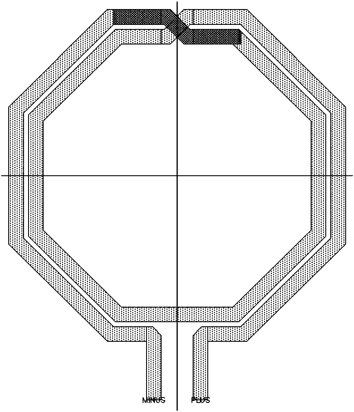
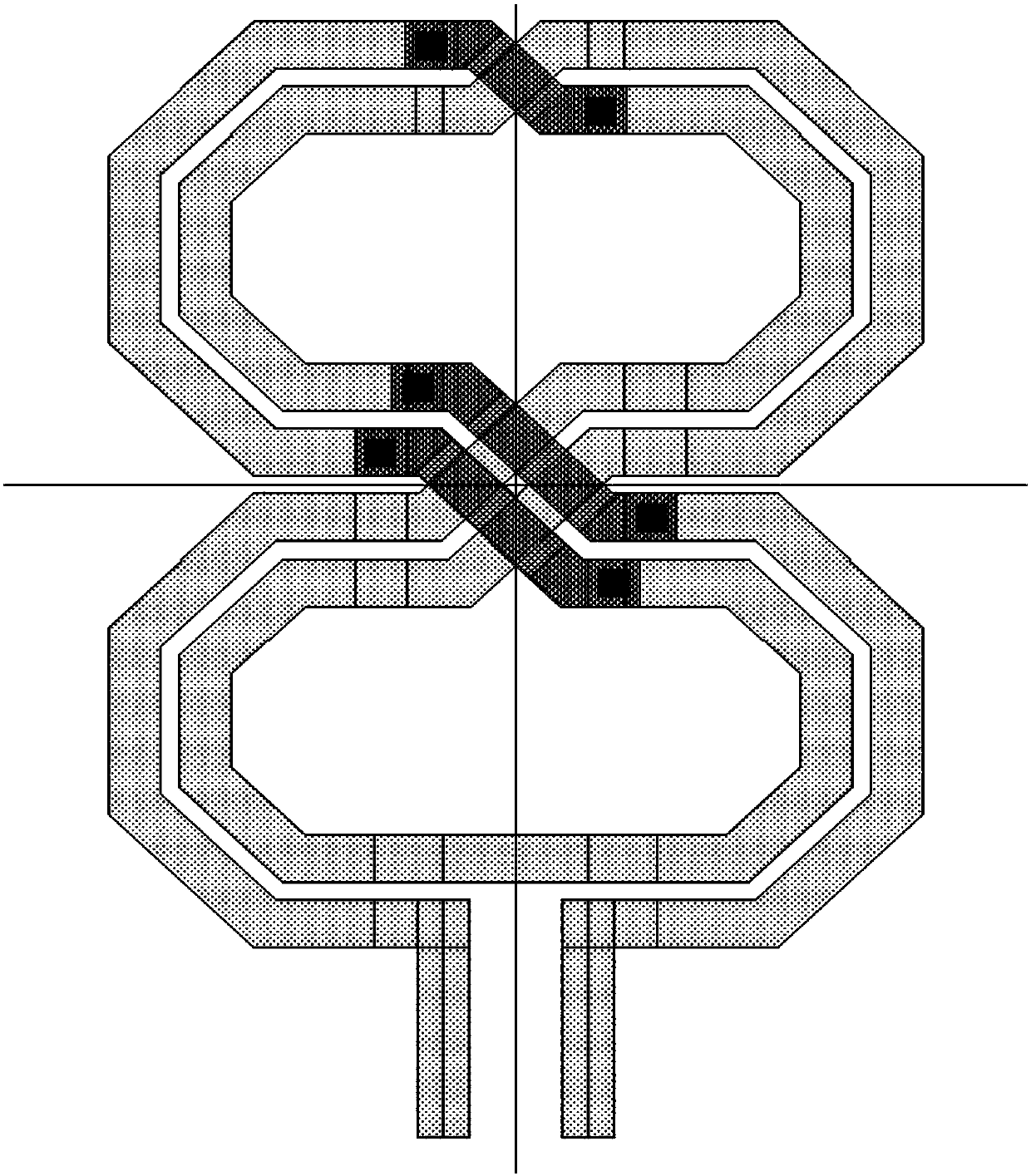
[0058] The present invention provides an integrated 8-shaped inductor structure on a semiconductor chip, including a jumper metal strip 51, a first helical coil 52 and a second helical coil 53, the first helical coil 52 and the second helical coil 53 The winding direction is the same; the first helical coil 52 includes a plurality of first sub-coils, the second helical coil 53 includes a plurali...


PUM

PropertyMeasurementUnit
Thicknessaaaaaaaaaa

Abstract

The invention is used in the field of microelectronics, and provides an 8-shaped inductor structure integrated on a semiconductor chip, and a semiconductor structure. The inductor structure comprisesa jumper metal strip arranged on a first metal layer, a first spiral coil arranged on a second metal layer and a second spiral coil arranged on the second metal layer, wherein winding directions of the first spiral coil and the second spiral coil are the same; a coil winding number of each of the first spiral coil and the second spiral coil is at least two, a starting point of the first spiral coil is connected with the first end of the jumper metal strip, a starting point of the second spiral coil is connected with the second end of the jumper metal strip, and an end point of the first spiralcoil is connected with an end point of the second spiral coil; and the outermost coil of the first spiral coil or the second spiral coil is provided with an opening, and the coils positioned on two ends of the opening serve as an input end and an output end of the 8-shaped inductor structure separately.

Description

technical field [0001] The invention belongs to the field of microelectronics, in particular to an 8-shaped inductance structure integrated on a semiconductor chip and a semiconductor structure. Background technique [0002] In the process of radio frequency integrated circuit (RFIC) voltage-controlled oscillator (VCO), it is very important to produce passive devices with high Q (Q is the quality factor of the inductor) value and resistance to interference. On-chip integrated inductors are passive components. The hardest part of the device to integrate. The use of high-Q and interference-resistant on-chip integrated inductors can greatly improve the stability of the VCO in the RFIC module and the efficiency of circuit design. In RFICs of silicon technology (CMOS and BiCMOS), due to the relatively low resistivity of the substrate, noise is easily coupled to the inductor coil through the substrate, resulting in poor stability of the inductor during operation and a decrease in...

Claims


Application Information

Patent Timeline
IPC IPC(8): H01L23/64
CPCH01L28/10
Inventor 黄志敏
Owner BUILDWIN SEMICON SHENZHEN CO LTD
Learn More