Welding method of multilayer copper-clad substrate of phased array active antenna array

A copper-clad substrate, active antenna technology, applied in welding equipment, auxiliary welding equipment, welding/cutting auxiliary equipment, etc. Accurate quantity control, meet production consistency, shorten the effect of production process

Active Publication Date: 2018-03-02
10TH RES INST OF CETC
View PDF9 Cites 4 Cited by
  • Summary
  • Abstract
  • Description
  • Claims
  • Application Information

AI Technical Summary

Problems solved by technology

[0006] For the selection of the shape of the solder, the current process method mainly relies on the lead-tin solder sheet to realize the application and control of the solder. The solder sheet needs to be laser cut to the shape of the welding cavity, and the cutting process causes secondary pollution. Even cleaning is difficult. The removal is clean, resulting in poor wetting effect between the substrate and the cavity, and large-area voids
The penetration rate is very limited. Due to the thick and large PTFE printed circuit board, the matching parameters between the amount of solder, welding pressure and welding time cannot be accurately controlled, which will cause a short circuit or low penetration rate, generally not higher than 50%. Unable to meet the high requirements for penetration and reliability of future high-frequency microstrip boards
[0007] The quality of step welding is uncontrollable. The large size, multi-layer active substrate and SMP RF connector 6 are not on the same welding surface. The step welding method is used for welding. The substrate and the front of the cavity are soldered by tin, silver and copper, and the cavity of SMP RF connector 6 is soldered by lead and tin. On the back, there are several flying problems: first, the wettability and diffusibility of tin-silver-copper solder are poor; second, the voids increase through secondary reflow soldering; For SMP tooling, the upper and lower layers of tooling are fixedly installed, resulting in an increase in the volume and thickness of the entire soldering, and an increase in soldering time. The silver plated layer of the substrate changes, the flux evaporates completely, and there is no exhaust channel. The welding process is also not visible
[0008] In terms of tooling design and installation sequence, the current tooling design mainly uses spring tooling to control the pressure, and the spring density is high, resulting in too large or too small pressure, the solder that is too large will overflow into the SMP hole, and the gap between the substrate and the cavity is too small. There are micro seams between them, resulting in poor welding
The second is the installation sequence of the tooling design. The substrate circuit faces upward, and the bonding state between the substrate welding surface and the cavity is basically impossible to judge. First, it leads to blind pressure.

Method used


Image

  • Welding method of multilayer copper-clad substrate of phased array active antenna array
  • Welding method of multilayer copper-clad substrate of phased array active antenna array

Examples


Embodiment Construction

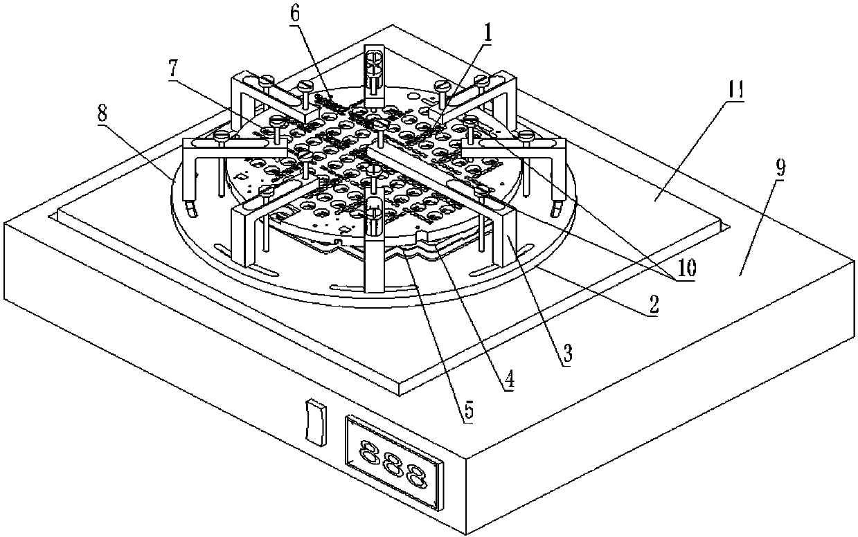
[0020] refer to figure 1 . According to the present invention, a tooling consistent with the shape of the contact surface of the multilayer copper-clad substrate 4 is prepared and its circular array is distributed on the L-shaped fixture 3 of the tooling base 2, and the long side of each L-shaped pointing to the center of the circle in the circumferential direction; The multi-layer copper clad substrate 4 is not on the same welding surface as the active circuit opening 7 and the packaged SMP radio frequency connector 6. The passive circuit faces downward, and the SMP soldering surface mounted on the surface faces upward. The multilayer copper clad substrate 4 and The non-metallic protection pad 5 is fixed on the raised surface of the tooling base 2, a solder ring, an SMP radio frequency connector 6 is placed in the SMP mounting hole on the reverse side of the cavity structure 8 and flux is applied, and a cotton ball 1 is used to block the SMP radio frequency connector 6 Insta...


PUM

PropertyMeasurementUnit
thicknessaaaaaaaaaa
diameteraaaaaaaaaa
diameteraaaaaaaaaa

Abstract

The present invention provides a welding method of a multilayer copper-clad substrate of a phased array active antenna array, and aims at providing a welding method capable of effectively preventing unstable welding quality of the multilayer copper-clad substrate. The welding method is implemented by the following technical scheme that a tool having the same shape with the multilayer copper-clad substrate and L-shaped clamps, an circular array of which is distributed on a tool pedestal, are prepared; steel mesh printing solder is applied to a front surface welding area of a cavity structural member and disposed on a reflux heating plate of a heater; the tool having the same shape with the multilayer copper-clad substrate and L-shaped clamps, the circular array of which is distributed on the tool pedestal, are prepared; the surface of the multilayer copper-clad substrate equipped with an SMP solder side is upward, the multilayer copper-clad substrate is fixed on a projection surface ofthe tool pedestal, solder rings and SMP radio frequency connectors are disposed in SMP installing holes in the reverse side of the cavity structural member, and soldering flux is applied; the back side of the multilayer copper-clad substrate is tinned, and the multilayer copper-clad substrate is fixed on the solder side of the cavity structural member coated with the soldering flux through pins and disposed on the reflux heating plate of the heater; and front surface welding of the multilayer copper-clad substrate and the cavity structural member is performed by hot reflux, and cavity back surface welding of the SMP radio frequency connectors to the cavity structural member is performed.

Description

technical field [0001] The invention relates to a phased array active antenna array 14mm×216mm×3.5mm large-scale multi-layer copper-clad substrate 4 welding tooling and an integrated welding process for a metal carrier and a radio frequency connector. Background technique [0002] With the rapid development of microelectronics technology and large-scale integrated circuits, the problem of making antennas a bulky and bulky part of electronic equipment has become prominent, and the demand for small antennas that can coordinate with the size of equipment and have effective electrical performance is becoming more and more urgent. Millimeter-wave phased array antennas are becoming thinner and thinner and are developing in the direction of conformal bending. The millimeter-wave two-dimensional active phased array antenna is characterized by large scale and high integration, which requires equipment miniaturization and adaptability to platform installation. Usually realize high-de...

Claims


Application Information

Patent Timeline
Patent Type & Authority Applications(China)
IPC IPC(8): B23K1/00B23K1/20B23K3/08B23K37/04
CPCB23K1/0016B23K1/20B23K1/203B23K3/087
Inventor 李颖凡林佳星何小峰林奈王文川陈中良
Owner 10TH RES INST OF CETC
Why Eureka
Try Eureka