A three-terminal magnetic random access memory and its reading and writing method

A technology of random access memory, reading and writing method, applied in static memory, digital memory information, information storage and other directions, can solve the problems of reducing the signal resolution ability of the storage unit, low signal resolution ability, etc., to improve the signal resolution ability, great application prospects Effect

Active Publication Date: 2021-10-29
CETHIK GRP +1
View PDF4 Cites 0 Cited by
  • Summary
  • Abstract
  • Description
  • Claims
  • Application Information

AI Technical Summary

Problems solved by technology

[0005] The purpose of the present invention is to provide a three-terminal magnetic random access memory and its reading and writing method. Aiming at the problem that the current two-terminal reading and writing electric field or stress-assisted STT-MRAM memory cell signal resolution is low, a method of improving The three-terminal STT-MRAM memory with high signal resolution and its reading and writing method solves the problem that the existing two-terminal reading and writing method reduces the signal resolution of the storage unit

Method used


Image

  • A three-terminal magnetic random access memory and its reading and writing method
  • A three-terminal magnetic random access memory and its reading and writing method
  • A three-terminal magnetic random access memory and its reading and writing method

Examples


Embodiment 1

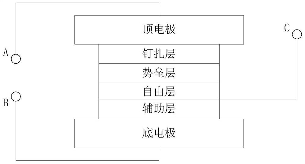
[0023] Such as Figure 2a As shown, the bottom electrode, auxiliary layer, free layer, barrier layer, pinning layer and top electrode are sequentially deposited on the silicon wafer (substrate) that has been prepared for the front-end process. On the free layer, a third terminal C is drawn out from the side that is in contact with the auxiliary layer. The magnetization direction of the pinned layer is fixed perpendicular to the film plane, and the magnetization direction of the free layer is variable.

[0024] By applying an electric field at the A and B terminals to change the magnetization direction of the free layer, the writing and erasing functions of the memory cell are realized. The resistance value of the memory cell is read by applying an electric field at the A and C terminals.

Embodiment 2

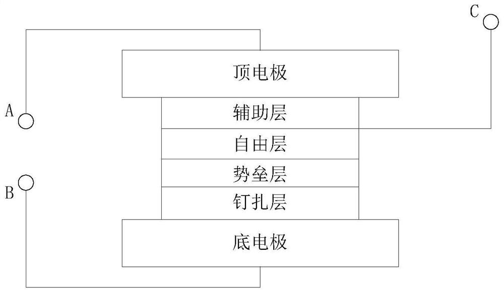
[0026] The order of the individual layers of the STT-MRAM stack can be reversed, as Figure 2b As shown, on the free layer, a third terminal C is led out from the side in contact with the auxiliary layer, and its properties have not changed. By applying an electric field at the A and B terminals to change the magnetization direction of the free layer, the writing and erasing functions of the memory cell are realized. The resistance value of the memory cell is read by applying an electric field at the B and C terminals.

Embodiment 3

[0028] Such as Figure 3a As shown, the difference from Embodiments 1 and 2 is that the magnetization direction of the pinned layer is fixed by the coupling between the antiferromagnetic coupling layer and the pinned layer. The bottom electrode, the auxiliary layer, the free layer, the barrier layer, the pinning layer, the antiferromagnetic coupling layer, the fixed layer and the top electrode are sequentially deposited on the silicon wafer that has been prepared for the front-end process. The magnetization direction of the pinned layer is fixed perpendicular to the film plane, and the magnetization direction of the free layer is variable. Likewise, on the free layer, a third terminal C is led out from the side that is in contact with the auxiliary layer. By applying an electric field at the A and B terminals to change the magnetization direction of the free layer, the writing and erasing functions of the memory cell are realized. The resistance value of the memory cell is r...


PUM


Abstract

The invention discloses a three-terminal magnetic random access memory and a reading and writing method thereof, which belong to the technical field of semiconductor storage. On the free layer of STT-MRAM assisted by stress and electric field, a third terminal is drawn out from the side contacting the auxiliary layer. Applying an electric field between the bottom and top electrodes enables the spin-transfer torque magneto-resistive random access memory to realize the write / erase function, and applying an electric field between the bottom or top electrode and the third terminal reads the stored state resistance. The three-terminal STT-MRAM proposed by the present invention does not pass through the auxiliary layer when reading the MTJ resistance state, thereby improving the signal resolution capability of the high and low resistance states of the MTJ memory unit, and has great application prospects.

Description

technical field [0001] The invention relates to the field of semiconductor memory, in particular to a three-terminal magnetic random access memory and a reading and writing method thereof. Background technique [0002] STT-MRAM memory is based on the change of the resistance state of the memory cell to achieve storage. It has the advantages of fast speed, non-volatility and long life. The basic memory cell includes a top electrode, a memory cell and a bottom electrode. A magnetic tunnel junction (MTJ) memory cell for STT-MRAM includes a free layer, a barrier layer, and a pinned layer. When the magnetization direction of the free layer is parallel / antiparallel to the magnetization direction of the pinned layer, the resistance state of the MTJ is in the low / high state, corresponding to the storage state 0 and 1, respectively. [0003] In order to reduce the power consumption of the entire device and prevent the breakdown of the barrier layer, the current of STT-MRAM during th...

Claims


Application Information

Patent Timeline
Patent Type & Authority Patents(China)
IPC IPC(8): H01L43/02H01L43/08H01L43/12G11C11/15
CPCG11C11/15H10N50/80H10N50/10H10N50/01
Inventor 左正笏喻涛陈志刚刘瑞盛刘波
Owner CETHIK GRP
Why Eureka
Try Eureka