
Lighting uniformity correction device, lighting uniformity correction method and exposure projection system

A uniformity correction and projection system technology, which is applied in the field of lithography lighting, can solve the problems affecting the production rate and the difficulty in the process of the variable gray compensation plate, so as to achieve the effects of increasing the production rate, maintaining the uniformity of the pupil, and reducing the cost

Inactive Publication Date: 2018-04-06
SHANGHAI MICRO ELECTRONICS EQUIP (GRP) CO LTD
View PDF10 Cites 7 Cited by
  • Summary
  • Abstract
  • Description
  • Claims
  • Application Information

AI Technical Summary

Problems solved by technology

[0008] The third solution is: in the early stage of the lighting system, a fixed gray scale compensation plate is used to eliminate the non-uniformity caused by the compensation structure of the variable shading head. However, with the increasing demand for lighting modes of the lithography lighting system, The fixed gray scale compensation plate cannot satisfy the uniformity optimization in the case of multiple lighting modes
[0009] At present, in the high NA front lighting system, there are dozens or even hundreds of lighting modes. It is difficult to make such a variable gray scale compensation plate compatible with the process, and the long-term problems caused by the uniformity of the lighting system and the objective lens system Drift and uniformity changes caused by pollution during use require a redesign of the variable gray scale compensation board every six months. Replacing the compensation board once will also affect the yield. It is necessary to propose a solution to the uniformity compensation and uniformity of multiple lighting modes. Solution for frequent replacement of variable gray scale compensation board caused by drift

Method used


Image

  • Lighting uniformity correction device, lighting uniformity correction method and exposure projection system
  • Lighting uniformity correction device, lighting uniformity correction method and exposure projection system
  • Lighting uniformity correction device, lighting uniformity correction method and exposure projection system

Examples


Embodiment 2

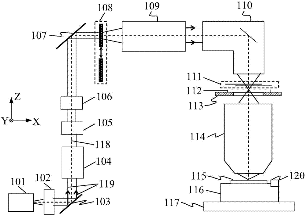
[0101] Please focus on reference Figure 13 The difference between this embodiment and Embodiment 1 is that the specific structure of the third module 110 is different. The third module 110 in this embodiment specifically includes a uniform light component, and the uniform light component in this embodiment adopts a quartz rod or a quartz rod Combination 601, combined with variable shading knife-edge array pair 602, variable knife-edge assembly 603, and condenser lens group 503, the light beam 119 is incident on the mirror array 504 after passing through the condenser lens group 503, and the pupil is imaged to the reticle 112 and illuminate the pattern on the reticle 112 . In order to obtain a trapezoidal illumination field distribution in the scanning direction (ie, the Y direction), the position of the reticle 112 deviates from the rear focal plane of the condenser lens group 503 , and this embodiment can also achieve the function of modulating the illumination light intensi...


PUM


Abstract

The invention relates to a lighting uniformity correction device, a lighting uniformity correction method and an exposure projection system. The lighting uniformity correction device comprises a variable light shielding correction device, a variable gray compensation plate device and a variable reflection mirror array device, wherein the variable light shielding correction device comprises a plurality of correction component pairs which are arranged on the cross section of a lighting beam; the plurality of the correction component pairs are arranged at intervals in a non-scanning direction tocover a whole lighting field and are overlapped in the scanning direction to cover the whole lighting field; the variable gray compensation plate device comprises two flat plates which can be moved relatively and have different gray transmittance rates; and the variable reflection mirror array device comprises a variable reflection mirror optical device; and the variable reflection mirror opticaldevice consists of a plurality of reflection mirror arrays with variable reflection rates. By adjusting the shapes and the overlapping modes of the component pairs, the transmittance rates of the flatplates and the reflection rates of the reflection mirror arrays, the lighting uniformity of the whole lighting field in multiple lighting modes is adjusted. By adopting the lighting uniformity correction device, the problems that gray compensation plates are frequently replaced, and properties of pupil uniformity and view field integral uniformity cannot be met in multiple lighting modes are solved.

Description

technical field [0001] The invention relates to the technical field of lithography illumination, in particular to an illumination uniformity correction device, a correction method and an exposure projection system. Background technique [0002] Photolithography is used in the manufacture of semiconductor devices. Photolithography uses electromagnetic radiation, such as ultraviolet (UV), deep UV, or visible light, to produce fine patterns in the design of semiconductor devices. Many types of semiconductor devices, such as diodes, transistors, and integrated circuits , can be fabricated by photolithography. A lithography exposure system usually includes an illumination system, a reticle containing a circuit pattern, a projection system, and a silicon wafer and a silicon wafer alignment stage for coating photoresist. The illumination system illuminates the circuit pattern on the reticle, and the projection system takes the An image of the illuminated area of ​​the circuit diag...

Claims


Application Information

Patent Timeline
Patent Type & Authority Applications(China)
IPC IPC(8): G03F7/20
CPCG03F7/70075G03F7/70358
Inventor 孙文凤
Owner SHANGHAI MICRO ELECTRONICS EQUIP (GRP) CO LTD
Learn More