

Method for preparing polycrystalline silicon thin film by infrared laser
A technology of polysilicon thin film and amorphous silicon thin film, which is applied in semiconductor/solid-state device manufacturing, electrical components, circuits, etc., can solve the problem of small grain size and achieve the effect of less defects and good crystallization effect
- Summary
- Abstract
- Description
- Claims
- Application Information
AI Technical Summary
Problems solved by technology
Method used
Image

Examples
Embodiment 1
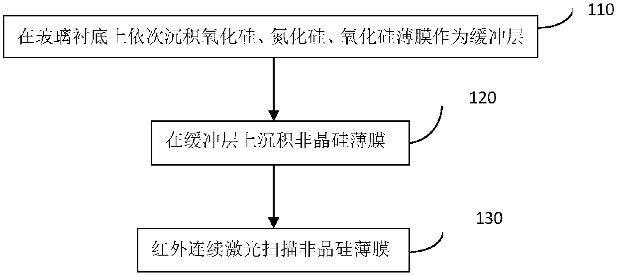
[0029] The embodiment of the present invention provides a method for preparing a polysilicon thin film with an infrared laser, such as figure 1 As shown, it specifically includes the following steps:
[0030] 110 sequentially deposit silicon oxide, silicon nitride, and silicon oxide thin films on the glass substrate as a buffer layer.
[0031] 120 depositing an amorphous silicon thin film on the buffer layer.
[0032] 130 scans the amorphous silicon film with a continuous laser.
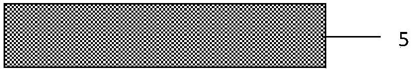
[0033] Among them, such as figure 2 The demonstrated substrate uses 3.3mm thick borosilicate glass, which has excellent thermal and optical properties.
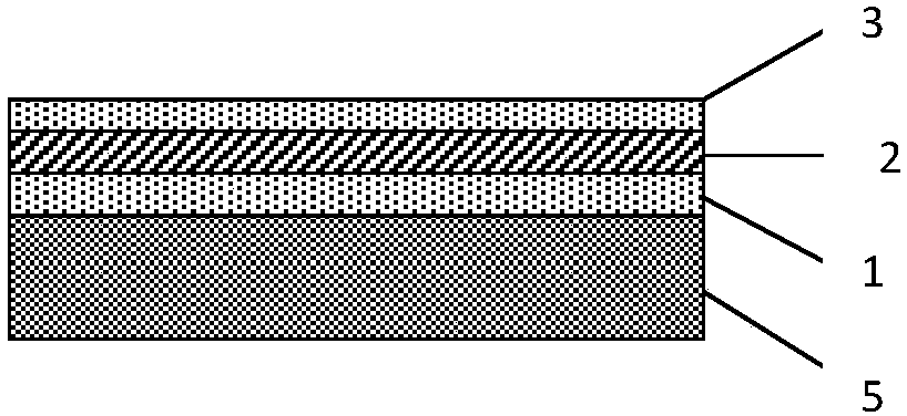
[0034] like image 3 As shown, 1: 80nm SiOx film, 2: 70nm SiNx film, 3: 15nm SiOx film are deposited sequentially on the glass substrate as a buffer layer. The buffer layer can be deposited by PECVD (Plasma Enhanced Chemical Vapor Deposition) plasma enhanced chemical vapor deposition Method deposition. The buffer layer composed of these three...
PUM
 Abstract
Description
Claims
Application Information