Airtight wafer level packaging structure and process of surface acoustic wave device

A surface acoustic wave device and wafer-level packaging technology, which is applied to electrical components, impedance networks, etc., can solve the problems of increasing size, achieve the effects of improved air tightness, high shear strength, and improved processing efficiency

Pending Publication Date: 2018-04-17
CETC CHIPS TECH GRP CO LTD
View PDF0 Cites 16 Cited by
  • Summary
  • Abstract
  • Description
  • Claims
  • Application Information

AI Technical Summary

Problems solved by technology

Since the internal leads need to be brought out of the package, the size of the package needs to be increased

Method used


Image

  • Airtight wafer level packaging structure and process of surface acoustic wave device
  • Airtight wafer level packaging structure and process of surface acoustic wave device

Examples


Embodiment Construction

[0031] The present invention will be described in detail below in conjunction with the accompanying drawings and specific embodiments.

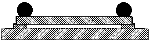
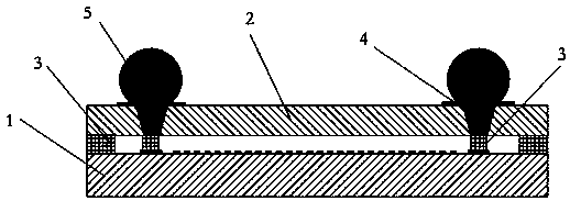
[0032] The packaging technology is applied in the technical field of packaging of high-reliability surface acoustic wave devices. Specifically, the functional chip of the surface acoustic wave device and the capping wafer are bonded together by wafer packaging technology to form an airtight seal.

[0033] The structure of the surface acoustic wave device targeted by this packaging process is as follows: figure 2 As shown, it can be seen from the figure that the surface acoustic wave device includes a functional chip 1 and a capping wafer 2, a circle of bonding layer metal 3 is plated on the periphery of the working surface of the functional chip 1, and the capping wafer 2 A circle of bonding layer metal 3 is also plated on the corresponding position of each chip bonding layer metal, and the functional chip 1 and the capping wafer 2 are bonde...


PUM


Abstract

The invention discloses a surface acoustic wave device airtight wafer-level packaging structure and technology. A ring of bonding layer metal is coated on the periphery of the working surface of a functional chip, and the sealing wafer corresponds to the bonding layer metal of each chip. A circle of bonding layer metal is plated on each position, and the functional chip and the cover wafer are combined together through gold-gold bonding or eutectic bonding; an external circuit wiring structure is provided on the side of the cover wafer facing away from the working surface of the functional chip and external electrodes; external solder balls are formed on the external electrodes; via holes are provided on the capping wafer to electrically connect the circuit on the working surface of the functional chip through the via holes, external electrodes and external solder balls in sequence. The invention can realize the airtight packaging of the wafer-level (WLP) surface acoustic wave device with high chip shearing strength, good heat dissipation and controllable internal atmosphere of the packaging, and has the characteristics of high reliability.

Description

technical field [0001] The invention relates to a surface acoustic wave device, in particular to an airtight wafer-level packaging structure and process for a surface acoustic wave device, and belongs to the technical field of surface acoustic wave device packaging. Background technique [0002] Surface acoustic wave (Surface Acoustic Wave, SAW) device is a frequency-selective device made of surface acoustic wave effect and resonance characteristics. Surface acoustic wave devices, especially surface acoustic wave filters (SurfaceAcoustic Wave Filter, SAWF) have small size, light weight, good consistency, high reliability, real-time signal processing, analog / digital compatibility, and anti-electromagnetic interference performance The advantages of good, low loss and good frequency selectivity have always been key devices in mobile communications and automotive electronics. With the continuous development of technology in the field of mobile communication and other fields, em...

Claims


Application Information

Patent Timeline
Patent Type & Authority Applications(China)
IPC IPC(8): H03H9/10
CPCH03H9/1064
Inventor 米佳朱勇冷俊林陶毅
Owner CETC CHIPS TECH GRP CO LTD
Why Eureka
Try Eureka