Manufacturing method of top gate type thin film transistor and top gate type thin film transistor

A technology of thin film transistor and manufacturing method, which is applied in transistor, semiconductor/solid-state device manufacturing, semiconductor device and other directions, can solve the problems of high manufacturing cost and complicated process flow, and achieve the effect of simplifying structure, reducing the number of manufacturing processes, and simple structure.

Active Publication Date: 2018-04-20
SHENZHEN CHINA STAR OPTOELECTRONICS SEMICON DISPLAY TECH CO LTD
View PDF2 Cites 7 Cited by
  • Summary
  • Abstract
  • Description
  • Claims
  • Application Information

AI Technical Summary

Problems solved by technology

[0005] In the manufacturing method of the above-mentioned top-gate thin film transistor, the patterning process of the active layer 200, the patterning process of the gate 400 and the gate insulating layer 300, the patterns of the interlayer dielectric layer 500, the source 610 and the drain 620 Therefore, the entire top-gate thin film transistor manufacturing process needs at least four masks to complete, the process flow is complicated, and the production cost is relatively high.

Method used


Image

  • Manufacturing method of top gate type thin film transistor and top gate type thin film transistor
  • Manufacturing method of top gate type thin film transistor and top gate type thin film transistor
  • Manufacturing method of top gate type thin film transistor and top gate type thin film transistor

Examples


Embodiment Construction

[0044] In order to further explain the technical means adopted by the present invention and its effects, the following describes in detail the preferred embodiments of the present invention and the accompanying drawings.

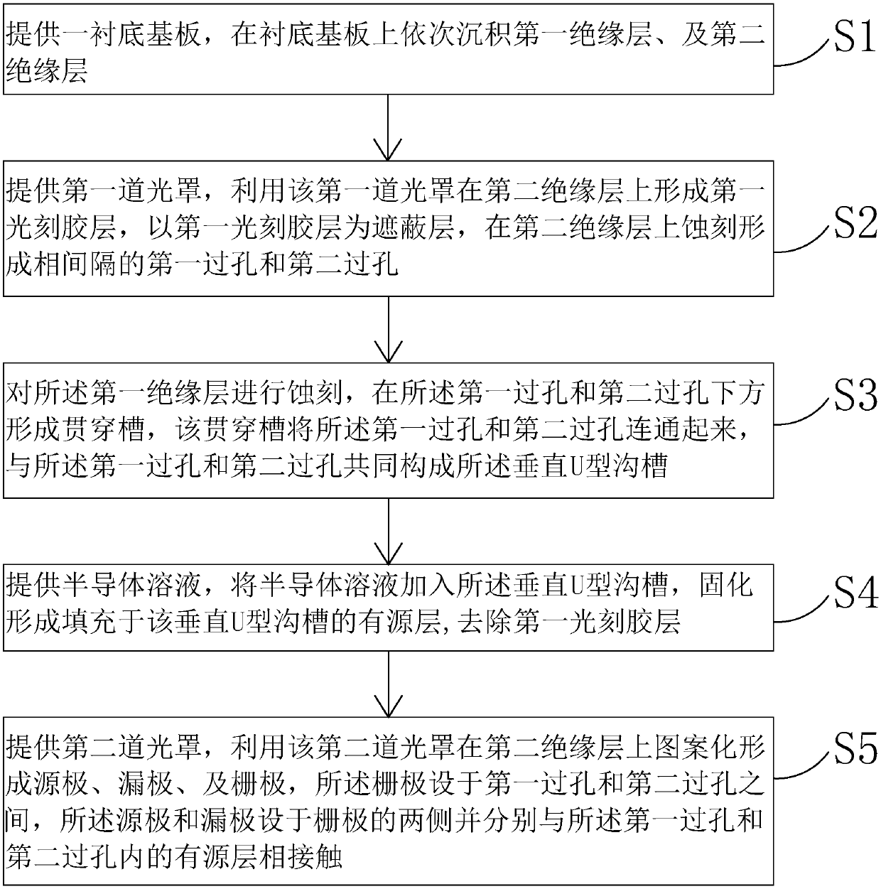
[0045] See figure 2 , The present invention first provides a method for manufacturing a top-gate thin film transistor, which includes the following steps:

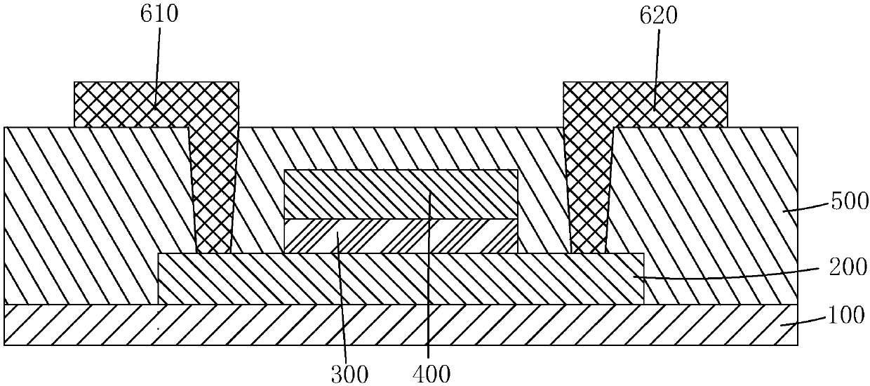
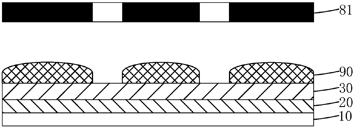
[0046] Step S1: Provide a base substrate 10, on which a first insulating layer 20 and a second insulating layer 30 with different dielectric constants and film material properties are sequentially deposited on the base substrate 10, for example, the lower layer The first insulating layer 20 can choose aluminum oxide (Al 2 O 3 ), hafnium dioxide (HfO 2 ), zirconium dioxide (ZrO 2 ), and the second insulating layer 30 on the upper layer can be silicon oxide (SiOx), silicon nitride (SiNx), etc.

[0047] Specifically, the first insulating layer 20 and the second insulating layer 30 are deposited by CVD (chemical v...


PUM


Abstract

The present invention provides a manufacturing method of a top gate type thin film transistor and a top gate type thin film transistor. The manufacturing method of the top gate type thin film transistor comprises the steps of: forming a first insulation layer and a second insulation layer on a substrate in order; employing a first photomask to form a first via hole and a second via hole which arearranged on the second insulation layer at intervals; forming a penetrating groove below the first via hole and the second via hole on the first insulation layer, wherein the penetrating groove is configured to communicate the first via hole with the second via hole, and the penetrating groove, the first via hole and the second via hole commonly form a vertical U-shaped groove; filling and formingan active layer in the vertical U-shaped groove; and employing a second photomask to form a source electrode, a drain electrode and a grid electrode on the second insulation layer. The manufacturingmethod of the top gate type thin film transistor and the top gate type thin film transistor simplifies the structure of the top gate type thin film transistor and reduces the number of photomask manufacture procedures, two photomasks are only used to complete manufacturing of the top gate type thin film transistor with the vertical U-shaped groove, and therefore, the process manufacturing cost issaved.

Description

Technical field [0001] The invention relates to the field of display technology, in particular to a method for manufacturing a top-gate thin film transistor and a top-gate thin film transistor. Background technique [0002] Thin Film Transistor (TFT) is currently the main switching element in liquid crystal display (Liquid Crystal Display, LCD) and Active Matrix Organic Light-Emitting Diode (AMOLED). It is directly related to the development direction of high-performance flat panel display devices. [0003] Thin film transistors have a variety of structures. The traditional bottom gate structure of thin film transistors, due to the large overlap area between the gate and the source and drain electrodes, produces a large parasitic capacitance, which will cause signal delay and the size of the manufactured thin film transistor Larger, thus limiting its application. The Top gate thin film transistor, because there is no overlap between the source and drain electrodes and the gate, i...

Claims


Application Information

Patent Timeline
Patent Type & Authority Applications(China)
IPC IPC(8): H01L29/786H01L21/336H01L21/34
CPCH01L29/66045H01L29/66969H01L29/78684H01L29/7869
Inventor 周志超夏慧陈梦
Owner SHENZHEN CHINA STAR OPTOELECTRONICS SEMICON DISPLAY TECH CO LTD
Why Eureka
Try Eureka