Wave absorbing and transmitting integrated metamaterial radome and application thereof
A technology of metamaterials and radomes, applied in the field of metamaterials, can solve problems such as loss of stealth ability, and achieve obvious effects of absorbing and transmitting waves.
- Summary
- Abstract
- Description
- Claims
- Application Information
AI Technical Summary
Problems solved by technology
Method used
Image
Examples
Embodiment 1
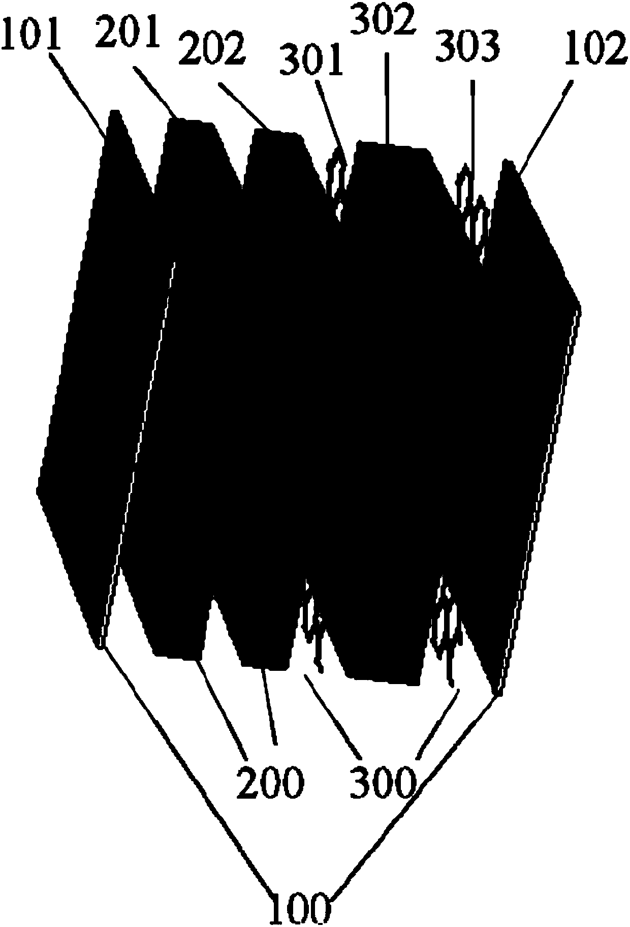
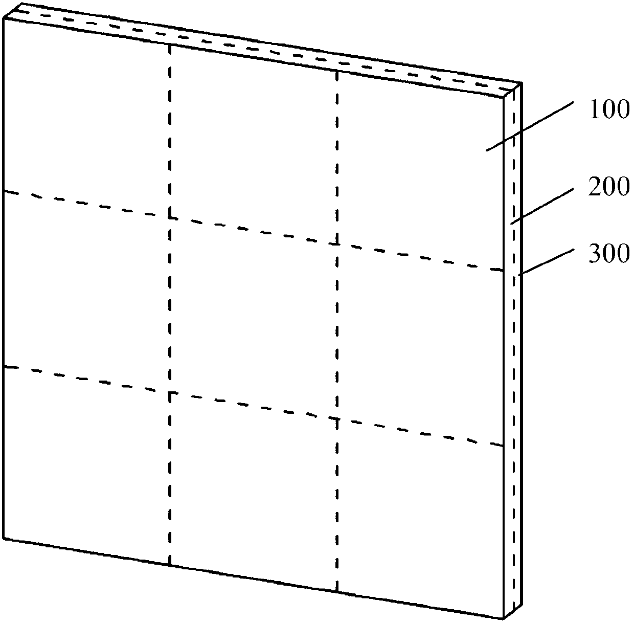
[0065] Please also refer to figure 1 and figure 2 , this embodiment provides an integrated metamaterial radome for absorbing and transmitting waves, which includes a dielectric structure layer 100 , a wave-absorbing sandwich layer 200 and a frequency-selective surface layer 300 .
[0066] The dielectric structure layer 100 includes a first dielectric substrate 101 and a second dielectric substrate 102, the first dielectric substrate 101 is arranged on one side of the wave-absorbing sandwich layer 200, and the frequency selective surface layer 300 is arranged on the side of the wave-absorbing sandwich layer 200 away from the second One side of the dielectric substrate 101 , the second dielectric substrate 102 is disposed on the side of the frequency selective surface layer 300 away from the absorbing core layer 200 .
[0067] The wave-absorbing sandwich layer 200 includes a first wave-absorbing sandwich layer 201 and a second wave-absorbing sandwich layer 202 . The first abs...
Embodiment 2
[0076] The difference between this embodiment and Embodiment 1 lies in that the thicknesses of the first dielectric substrate and the second dielectric substrate are both 3 mm. Both the first dielectric substrate and the second dielectric substrate are made of epoxy resin and glass fiber.
[0077] Both the first wave-absorbing sandwich layer and the second wave-absorbing sandwich layer are composed of wave-absorbing honeycombs, and the thicknesses of the first wave-absorbing sandwich layer and the second wave-absorbing sandwich layer are both 20mm.
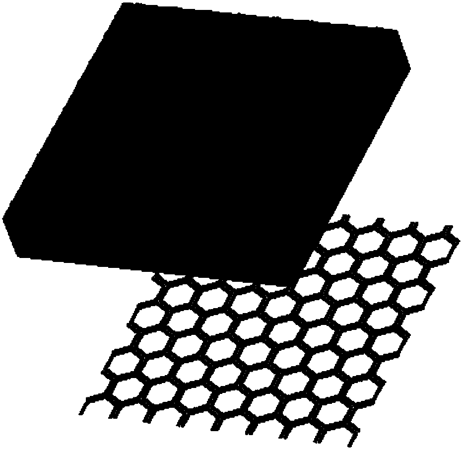
[0078] The side lengths of the hollow regular hexagonal metals of the first metal layer and the second metal layer are both 2 mm, and the widths of the hollow regular hexagonal metals of the first metal layer and the second metal layer are both 0.2 mm. The metals in the first metal layer and the second metal layer are both copper.
[0079] The third dielectric substrate is made of aramid paper honeycomb, and the thickness of the ...
Embodiment 3
[0081] The difference between this embodiment and Embodiment 1 is that the thicknesses of the first dielectric substrate and the second dielectric substrate are both 2 mm. Both the first dielectric substrate and the second dielectric substrate are made of vinyl ester resin, cyanate resin, quartz fiber and kevlar fiber.
[0082] Both the first wave-absorbing sandwich layer and the second wave-absorbing sandwich layer are composed of wave-absorbing foam, and the thicknesses of the first wave-absorbing sandwich layer and the second wave-absorbing sandwich layer are both 15 mm.
[0083] The side lengths of the hollow regular hexagonal metals of the first metal layer and the second metal layer are both 3 mm, and the widths of the hollow regular hexagonal metals of the first metal layer and the second metal layer are both 0.4 mm.
[0084] The third dielectric substrate is made of PMI foam, and the thickness of the third dielectric substrate is 10 mm.
PUM
 Abstract
Description
Claims
Application Information


