Three-dimensional memory formation method

A memory, three-dimensional technology, applied in semiconductor devices, electric solid-state devices, electrical components, etc., can solve the problems of increasing the production cycle and production cost of three-dimensional memory, complicated operations, increasing structural shape changes and structural size changes, and shortening production. effect of cycle time, simplified operation steps, reduced risk of structural damage

Active Publication Date: 2019-01-01
YANGTZE MEMORY TECH CO LTD
View PDF4 Cites 0 Cited by
  • Summary
  • Abstract
  • Description
  • Claims
  • Application Information

AI Technical Summary

Problems solved by technology

It can be seen from the above that in the formation process of the top select gate structure and the self-aligned structure of the last gate, it is necessary to form a photoresist layer, and all need to perform etching process, ashing process and wet cleaning process cycle, but the same operation is Performing it twice not only cumbersome operation, but also increases the production cycle and production cost of the three-dimensional memory, and increases the risk of structural shape changes and structural size changes caused by improper etching.

Method used


Image

  • Three-dimensional memory formation method
  • Three-dimensional memory formation method
  • Three-dimensional memory formation method

Examples


Embodiment Construction

[0028] Exemplary embodiments of the present disclosure will be described in more detail below with reference to the accompanying drawings. Although exemplary embodiments of the present disclosure are shown in the drawings, it should be understood that the present disclosure may be embodied in various forms and should not be limited by the embodiments set forth herein. Rather, these embodiments are provided for more thorough understanding of the present disclosure and to fully convey the scope of the present disclosure to those skilled in the art.

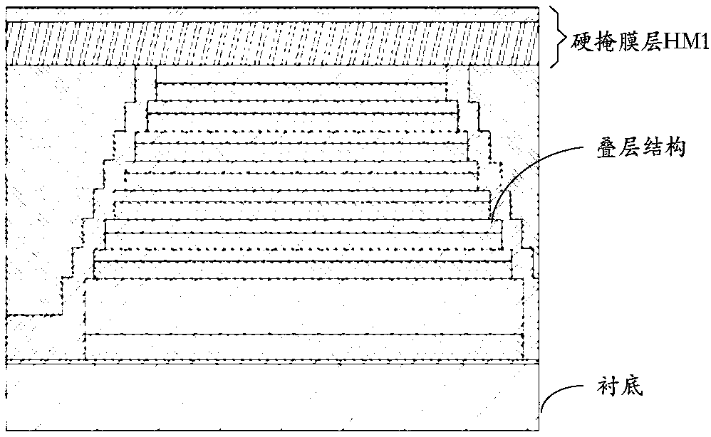
[0029] According to an embodiment of the present invention, a method for forming a three-dimensional memory is proposed, such as Figure 9 shown, including:

[0030] Provide a substrate, and form a stacked structure and a cutting line (Scrubber Line) on the substrate;

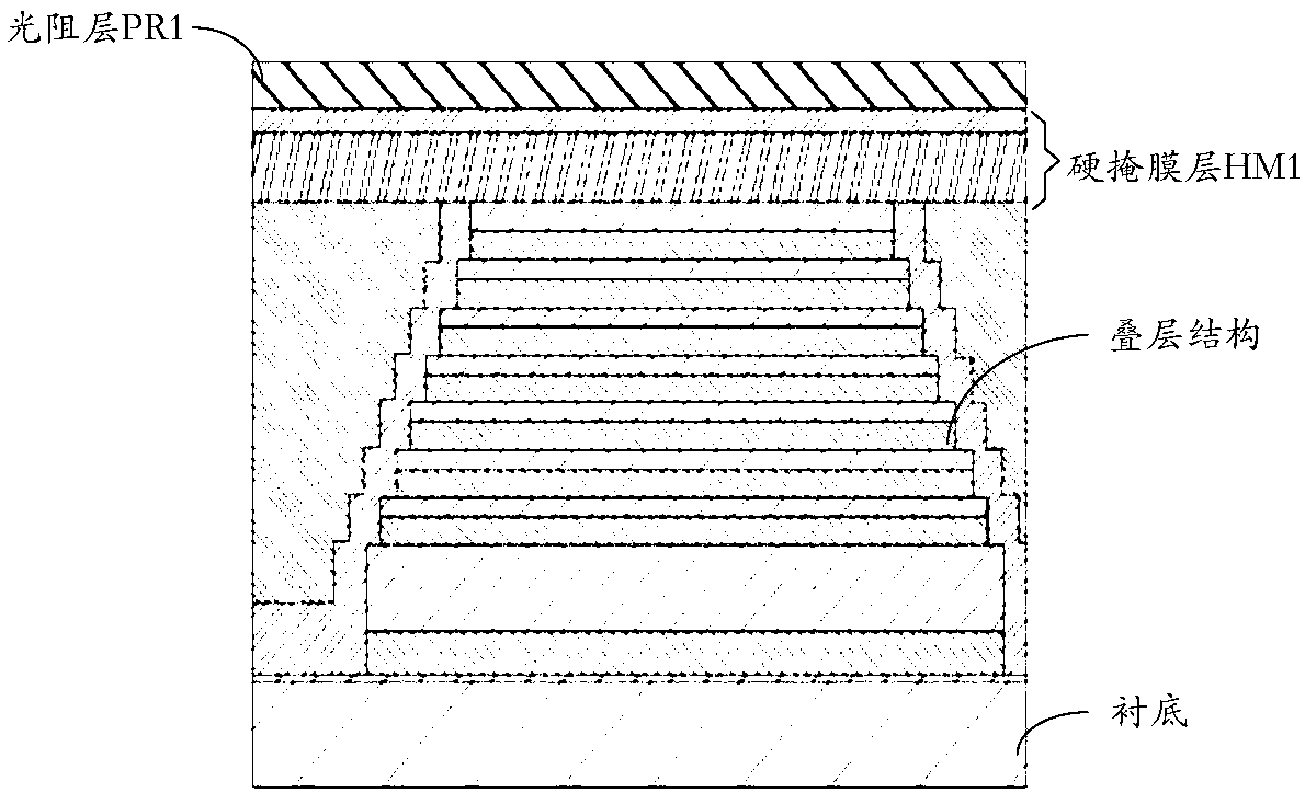
[0031] forming a first hard mask layer (Hard Mask) on the laminated structure and the dicing line;

[0032] forming a photoresist layer (Photo Resist) on the firs...


PUM


Abstract

The invention discloses a method for forming a three-dimensional memory, which belongs to the technical field of semiconductors. The method includes: providing a substrate, forming a stacked structure and a cutting line on the substrate; forming a first hard mask layer on the stacked structure and the cutting line; forming a photoresist layer on the first hard mask layer; Using the photoresist layer as a mask to etch the first hard mask layer and the stacked structure to form a first groove, and etch the first hard mask layer and the cutting line to form a second groove; in the first groove and the second Oxide with a predetermined thickness is deposited in the groove to form a corresponding top layer selection gate structure and a rear gate self-alignment structure; after forming a second hard mask layer by self-alignment on the rear gate self-alignment structure, a channel hole is formed. In the present invention, the fabrication of the top selection gate structure and the self-alignment structure of the back gate is carried out simultaneously, which not only simplifies the operation steps, shortens the production cycle of the three-dimensional memory, saves the production cost, but also reduces the Risk of structural damage and increased utilization of lithography equipment.

Description

technical field [0001] The invention relates to the technical field of semiconductors, in particular to a method for forming a three-dimensional memory. Background technique [0002] Three-dimensional memory is a new type of product based on planar memory. Its main feature is to convert the planar structure into a three-dimensional structure to greatly save the chip area. The formation of a three-dimensional memory involves thousands of operations and processes, among which the lithography process accounts for a certain proportion and is a large expense. Representatively, such as the top select gate structure (Top Select Gate (TSG for short) formation and Gate Last Self Align (GLSA for short) formation. In the existing method for forming a three-dimensional memory, the top select gate structure and the rear gate self-aligned structure are formed separately. Among them, the top select gate structure is formed first, such as Figure 1 to Figure 5 As shown, it usually mainly ...

Claims


Application Information

Patent Timeline
Patent Type & Authority Patents(China)
IPC IPC(8): H01L27/11519H01L27/11551H01L27/11565H01L27/11578
CPCH10B41/10H10B41/20H10B43/10H10B43/20
Inventor 张若芳刘藩东何佳魏毅朱喜峰王鹏夏志良霍宗亮
Owner YANGTZE MEMORY TECH CO LTD
Why Eureka
Try Eureka