BCD technology based high-sensitivity fingerprint sensor

A fingerprint sensor, high-sensitivity technology, applied in the direction of acquiring/arranging fingerprints/palmprints, instruments, characters and pattern recognition, etc., can solve the problems of increasing system cost, complex system structure, inconvenient installation, etc., and achieve volume and cost saving , Simplify the system, improve the effect of reliability

Pending Publication Date: 2018-05-11
深圳市凤浴科技有限公司
View PDF7 Cites 2 Cited by
  • Summary
  • Abstract
  • Description
  • Claims
  • Application Information

AI Technical Summary

Problems solved by technology

At the same time, there is a problem of inconvenient installation when the sensor with the metal ring is attached to the system-level machine shell during installation.
In the substrate driving scheme, DCDC and high-voltage interface chips will consume high power consumption at the system level, increasing the cost of the system; at the same time, the system structure is complex and debugging is inconvenient

Method used


Image

  • BCD technology based high-sensitivity fingerprint sensor
  • BCD technology based high-sensitivity fingerprint sensor
  • BCD technology based high-sensitivity fingerprint sensor

Examples


Embodiment Construction

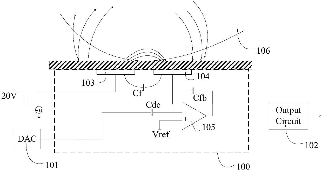
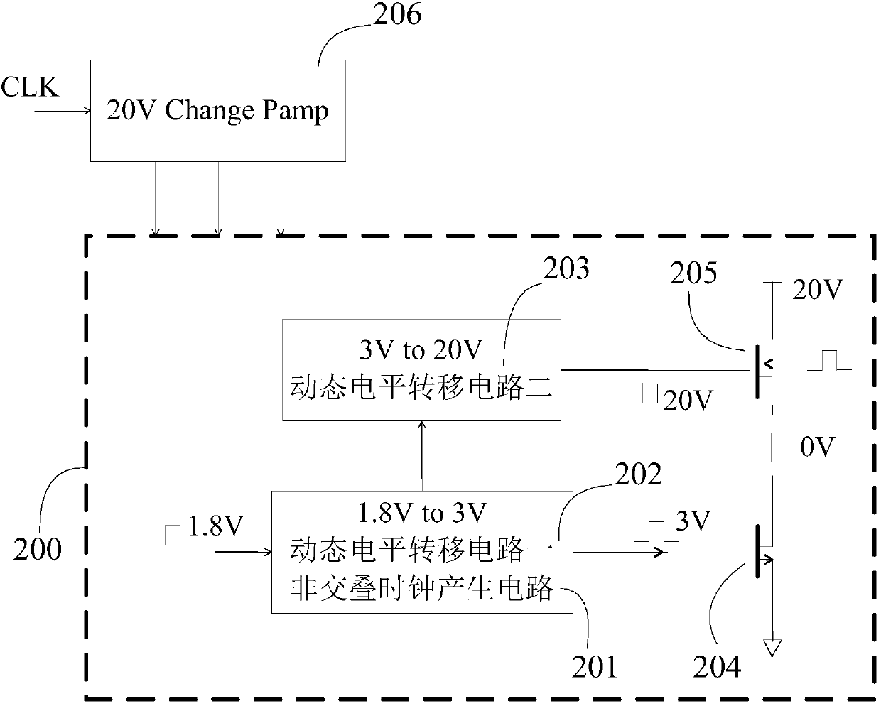
[0024] In order to make the objectives, technical solutions and advantages of the present invention clearer, the preferred embodiments of the present invention will be described below with reference to the accompanying drawings. A capacitive fingerprint sensor formed by an array of capacitive sensing elements is taken as an example to describe this patent in detail. , The capacitive sensing element array includes two or more fingerprint collection units. figure 2 It is a fingerprint collection unit circuit based on fringe electric field finger capacitance and high-voltage pulses in an embodiment of the present invention. image 3 It is the high-voltage pulse generating circuit of the embodiment of the present invention. Figure 4 It is the charge pump boost circuit of the embodiment of the present invention.

[0025] The high-sensitivity fingerprint sensor based on the BCD process proposed by the present invention includes: a fingerprint acquisition unit circuit 100, a high-volta...


PUM


Abstract

The invention provides a BCD technology based high-sensitivity fingerprint sensor which comprises a fingerprint collection unit circuit, a high-voltage pulse generating circuit and an internal boost circuit. The input end of the fingerprint collection unit circuit is connected with the high-voltage pulse generating circuit and a digital to analog converter, and the output end of the fingerprint collection unit circuit is connected with an output circuit or a post reception amplification circuit; the output end of the high-voltage pulse generating circuit is connected with the fingerprint collection unit circuit, and outputs a high-voltage excitation signal to the fingerprint collection unit to drive formation of fingerprints directly or indirectly; and the output end of the internal boostcircuit is connected with the high-voltage pulse generating circuit, and used to rise a relatively low voltage provided by a power supply to a relatively high voltage, and input a high voltage to thehigh-voltage pulse generating circuit. The fingerprint sensor uses the internal boost circuit, the excitation signal is generated in the circuit and acted on the internal of a chip, and thus, the detection sensitivity of the sensor can be improved effectively while a pricking feeling is not generated in the finger surfaces.

Description

Technical field [0001] The present invention relates to the technical field of fingerprint identification, in particular to a high-sensitivity fingerprint sensor based on BCD technology. Background technique [0002] Most of the existing fingerprint sensors use the sensor to generate an excitation signal. The excitation signal is applied to the surface of the finger to be collected by installing a metal ring around the sensor and touching the metal ring with the finger to be collected to realize the principle of driving the finger electrode Realize fingerprint collection, such as figure 1 (a) Shown. In the existing fingerprint sensor using the principle of finger excitation, in order to prevent some people from causing a tingling sensation during fingerprint collection, the maximum pulse excitation voltage on the finger generally does not exceed 4V. [0003] In addition, some of the existing sensors use high-voltage excitation signals to drive the fingerprint sensor substrate to a...

Claims


Application Information

Patent Timeline
Patent Type & Authority Applications(China)
IPC IPC(8): G06K9/00
CPCG06V40/1306
Inventor 李富民
Owner 深圳市凤浴科技有限公司
Why Eureka
Try Eureka