Laminated white light emitting diode based on quantum dot electroluminescence and preparation method thereof
A technology of light-emitting diodes and electroluminescence, applied in circuits, electrical components, electro-solid devices, etc., can solve the problems of low efficiency and poor spectral stability of white light devices
- Summary
- Abstract
- Description
- Claims
- Application Information
AI Technical Summary
Problems solved by technology
Method used
Image
Examples
Embodiment 1
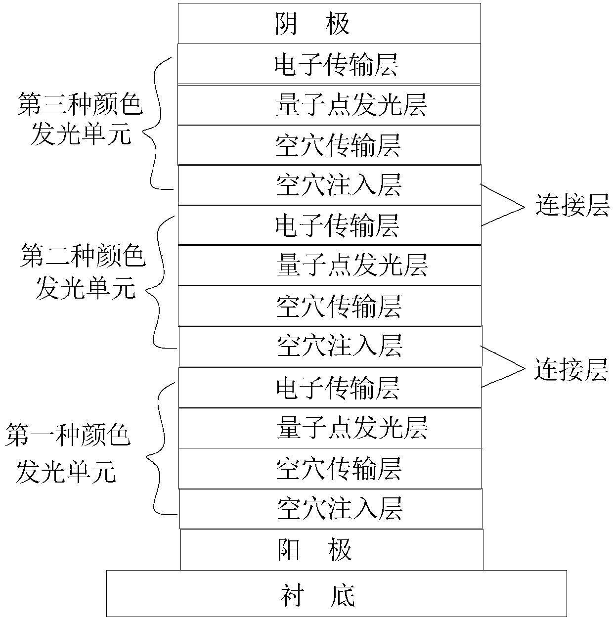
[0035] A stacked white light-emitting diode based on quantum dot electroluminescence, such as figure 1 As shown, it is composed of an anode, a cathode, and red, green, and blue light-emitting units stacked between the anode and the cathode. The arrangement order of the red, green and blue light-emitting units can be changed arbitrarily, and can be arranged according to red, green and blue from bottom to top, or can be arranged in green, blue and red, blue, red and green or other ways.
[0036] The two adjacent functional layers between two adjacent light-emitting units are connecting layers, and the connecting layer is composed of an electron transport layer in the lower light-emitting unit and a hole injection layer in the upper light-emitting unit.
[0037] The hole injection layer as the connection layer is a polyoxometalate film, and the electron transport layer as the connection layer is an n-type metal oxide nano particle film. The polyoxometalate is at least one of mol...
Embodiment 2
[0048] The present invention will be further described with a specific example.
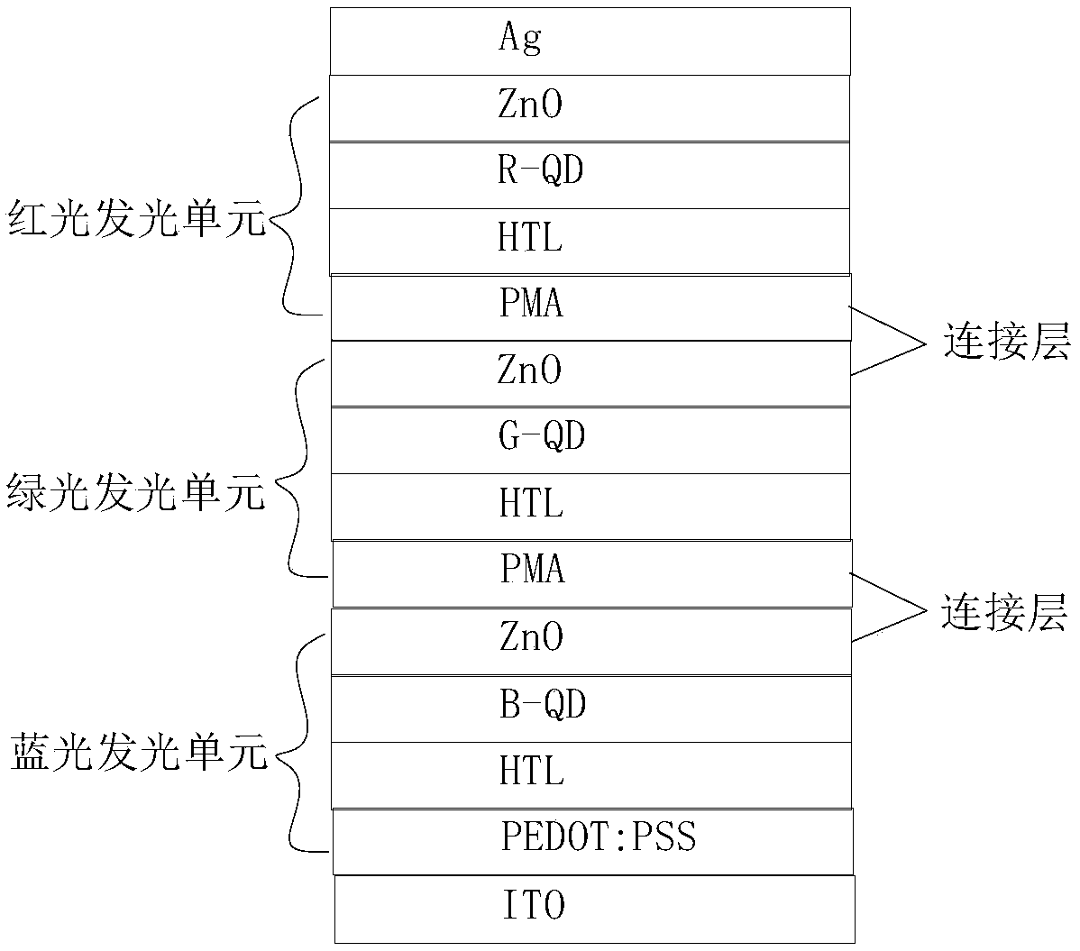
[0049] The device structure of this embodiment is: anode (ITO) / hole injection layer (PEDOT:PSS) / hole transport layer (HTL) / blue light emitting layer (B-QD) / electron transport layer (ZnO) / hole injection layer (phosphomolybdic acid-PMA) / hole transport layer (HTL) / green light emitting layer (G-QD) / electron transport layer (ZnO) / hole injection layer (phosphomolybdic acid-PMA) / hole transport layer (HTL) / red light-emitting layer (R-QD) / electron transport layer (ZnO) / cathode (silver-Ag), such as figure 2 shown.
[0050] The preparation process is as follows:
[0051] a. Put the ITO substrate used in tetrahydrofuran, isopropanol, washing solution, and deionized water for ultrasonic cleaning, and the ultrasonic time for each time is 10-20min. After the ultrasound is completed, place the ITO substrate in an oven to dry for later use.
[0052] b. Before the first hole injection layer (PEDOT:PSS) is pro...
Embodiment 3
[0060] The present invention will be further described with a specific example.
[0061] The device structure of this embodiment is: anode (graphene) / hole injection layer (phosphomolybdic acid-PMA) / hole transport layer (HTL) / green light emitting layer (G-QD) / electron transport layer (ZnO) / Hole injection layer (phosphomolybdic acid-PMA) / hole transport layer (HTL) / blue light emitting layer (B-QD) / electron transport layer (ZnO) / hole injection layer (phosphomolybdic acid-PMA) / hole Hole transport layer (HTL) / red light emitting layer (R-QD) / electron transport layer (ZnO) / cathode (silver-Ag), such as Figure 4 shown.
[0062] The preparation process is as follows:
[0063] a. Clean the graphene substrate in tetrahydrofuran, isopropanol, washing solution, and deionized water in sequence, and the ultrasonic time is 10-20 minutes each time. After the ultrasound is completed, place the graphene substrate in an oven to dry for later use.
[0064] b. before the first hole injection la...
PUM
 Abstract
Description
Claims
Application Information


