

Semiconductor device
一种半导体、元件的技术,应用在半导体元件领域,能够解决制作工艺复杂化等问题
- Summary
- Abstract
- Description
- Claims
- Application Information
AI Technical Summary
Problems solved by technology
Method used
Image

Examples
Embodiment Construction
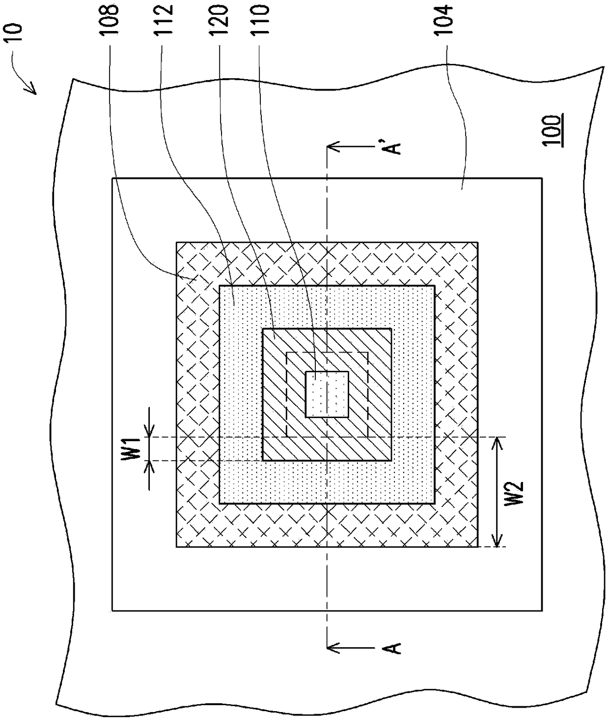
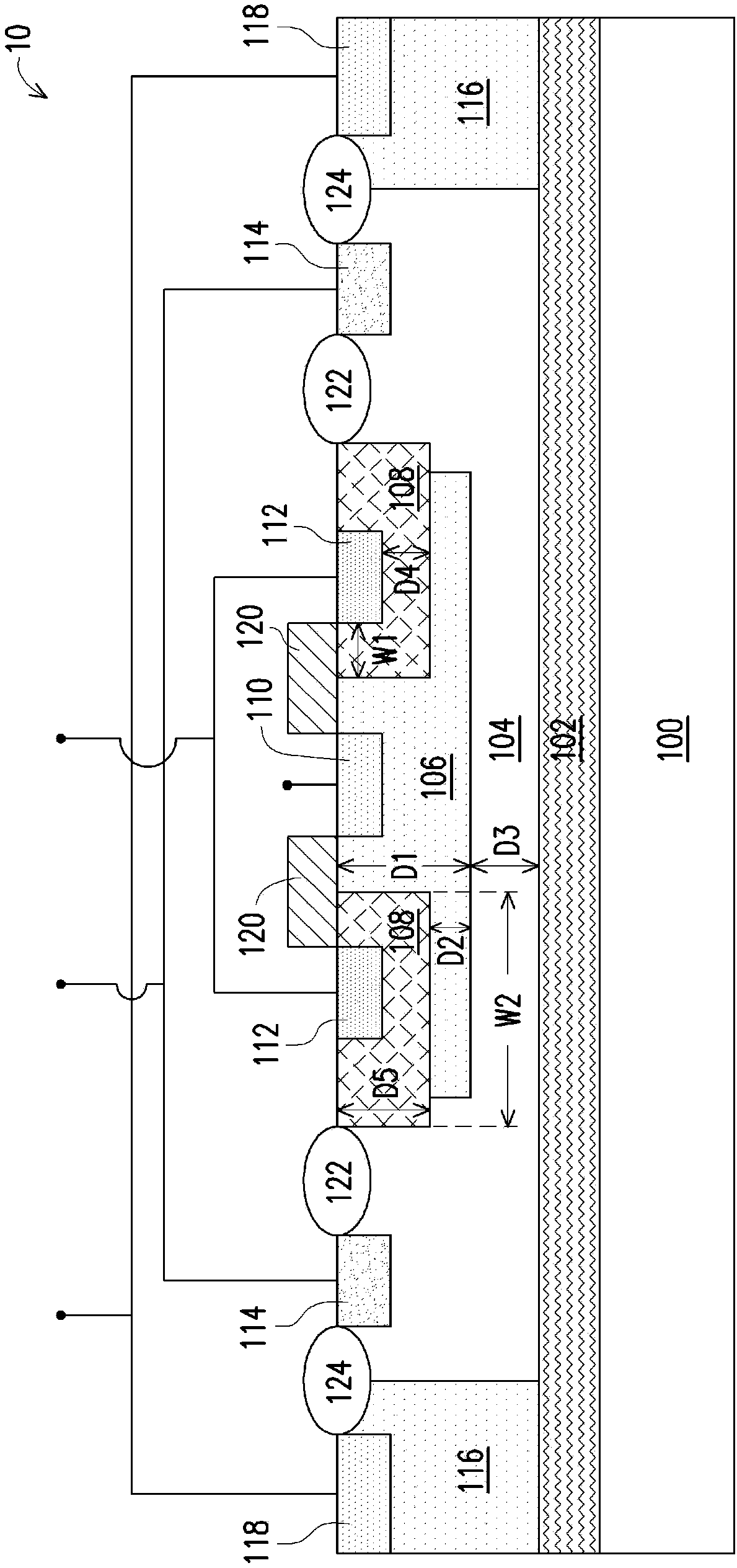
[0045] The present invention will be described more fully with reference to the drawings of this embodiment. However, the present invention can also be embodied in various forms and should not be limited to the embodiments described herein. The thicknesses of layers and regions in the drawings may be exaggerated for clarity. The same or similar symbols indicate the same or similar elements, and the following paragraphs will not repeat them one by one.
[0046] In the following embodiments, the first conductivity type is different from the second conductivity type. In one embodiment, the first conductivity type is N type, and the second conductivity type is P type. In another embodiment, the first conductivity type is P-type, and the second conductivity type is N-type. The P-type dopant is, for example, boron; the N-type dopant, for example, is phosphorus or arsenic. In this embodiment, the first conductivity type is P-type and the second conductivity type is N-type as an e...
PUM
 Abstract
Description
Claims
Application Information