Temperature-drift-free on-chip integrated laser and preparation method thereof

An integrated laser and temperature drift technology, which is applied in the structure of optical resonator cavity, structure of optical waveguide semiconductor, etc., can solve the problems of low power consumption of on-chip integrated laser, change of output wavelength with temperature, low preparation cost, etc., and achieves practicability. Strong, reduce power consumption, improve the effect of coupling efficiency

Inactive Publication Date: 2018-06-05
WUHAN POST & TELECOMM RES INST CO LTD
View PDF5 Cites 10 Cited by
  • Summary
  • Abstract
  • Description
  • Claims
  • Application Information

AI Technical Summary

Problems solved by technology

[0006] Aiming at the defects existing in the prior art, the object of the present invention is to provide a temperature-drift-free on-chip integrated laser and its preparation method, which can solve the problem that the emission waveleng

Method used


Image

  • Temperature-drift-free on-chip integrated laser and preparation method thereof
  • Temperature-drift-free on-chip integrated laser and preparation method thereof
  • Temperature-drift-free on-chip integrated laser and preparation method thereof

Examples


Embodiment 1

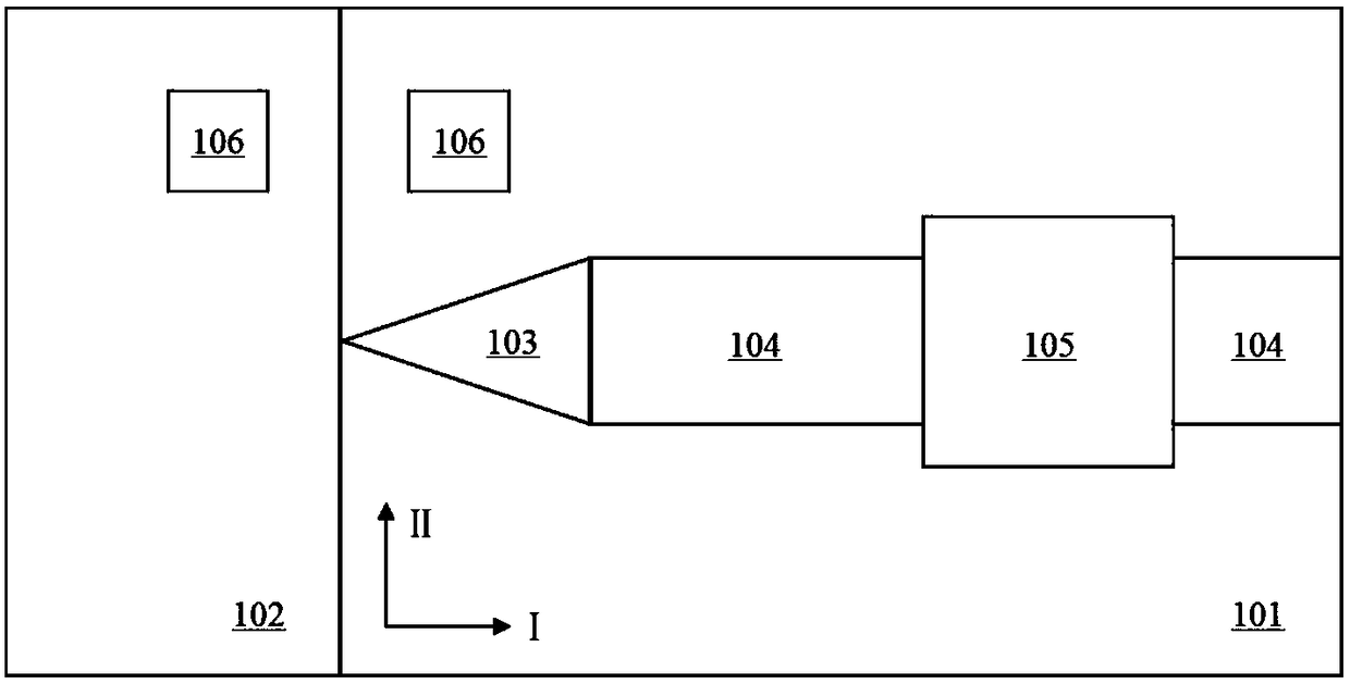
[0051] see Figure 1 to Figure 3 As shown, Embodiment 1 provides an on-chip integrated laser without temperature drift, including a low-refractive index substrate 101, a gain medium 102, a mode spot converter 103, a hybrid integrated optical waveguide 104 without temperature drift, and an optical waveguide without temperature drift. Resonant cavity 105 and a pair of alignment marks 106 . Wherein, the gain medium 102 is a quantum well structure based on the InGaAsP / InP material system, and realizes stimulated emission by electric pumping. The mode speckle converter 103 adopts an inverted tapered waveguide structure, and couples the light wave output by the gain medium 102 into the hybrid integrated optical waveguide 104 without temperature drift, and couples it into the optical resonant cavity 105 without temperature drift to realize the frequency selection function. A total reflection mirror is arranged on one side of the gain medium 102, and the total reflection mirror toget...

Embodiment 2

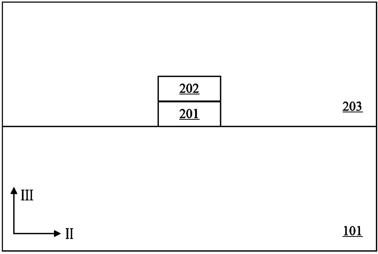
[0054] see Figure 4 with Figure 5 As shown, Embodiment 2 provides an on-chip integrated laser without temperature drift, and its basic structure is the same as that of Embodiment 1, except that: see Figure 4 As shown, the hybrid integrated optical waveguide 104 without temperature drift adopts a slit waveguide structure, including a high-refractive-index material layer 201 formed on a low-refractive-index substrate 101; The optical coefficient material layer 202 ; the low refractive index covering layer 203 formed on the negative thermo-optic coefficient material layer 202 . The materials of the low-refractive-index substrate 101 and the low-refractive-index cover layer 203 are both silicon dioxide, with a refractive index of 1.444 and a thermo-optic coefficient of 1.0*10 -5 K -1 ; The material of the high refractive index material layer 201 is silicon, the refractive index is 3.45, and the thermo-optic coefficient is 1.84*10 - 4 K -1 ; The material of the negative th...

Embodiment 3

[0056] see Image 6 As shown, Embodiment 3 provides an on-chip integrated laser without temperature drift, and its basic structure is the same as that of Embodiment 1, except that: see Image 6 As shown, the hybrid integrated optical waveguide 104 without temperature drift adopts a sub-wavelength grating waveguide structure, including a periodically arranged high refractive index material layer 201 formed on a low refractive index substrate 101; formed on the high refractive index material layer 201 The negative thermo-optic coefficient material layer 202 arranged periodically in the middle; the low refractive index covering layer 203 formed on the negative thermo-optic coefficient material layer 202 . The materials of the low-refractive-index substrate 101 and the low-refractive-index cover layer 203 are both silicon dioxide, with a refractive index of 1.444 and a thermo-optic coefficient of 1.0*10 -5 K -1 ; The material of the high refractive index material layer 201 is si...


PUM

PropertyMeasurementUnit
Widthaaaaaaaaaa
Thermo-optic coefficientaaaaaaaaaa

Abstract

The invention discloses a temperature-drift-free on-chip integrated laser and a preparation method thereof and relates to the technical field of electronic devices. The temperature-drift-free on-chipintegrated laser comprises a gain medium, a spot-size converter, an alignment mark, a temperature-drift-free hybrid integrated optical waveguide and a temperature-drift-free optical resonator, whereinthe gain medium is connected with the temperature-drift-free hybrid integrated optical waveguide through the spot-size converter; the temperature-drift-free hybrid integrated optical waveguide comprises high-refractive-index material layer formed on a low-refractive-index substrate and a negative-thermo-optical-coeffecient material layer which can compensate for a positive thermo-optical coefficient of the high-refractive-index material layer; and the temperature-drift-free optical resonator is of a resonator structure formed based on the temperature-drift-free hybrid integrated optical waveguide, and is used for stabilizing output wavelengths of the laser at different temperatures. The problem that an output wavelength of a silicon-based on-chip integrated laser changes with the temperature is solved. An additional regulation and control device does not need to be added, so that the temperature-drift-free on-chip integrated laser is low in power consumption, high in integration degree and low in preparation cost.

Description

technical field [0001] The invention relates to the technical field of optoelectronic devices, in particular to an on-chip integrated laser without temperature drift and a preparation method thereof. Background technique [0002] The rapid development of information technology has put forward higher and higher requirements for the transmission rate and integration of communication systems. Based on the characteristics of low loss, high refractive index difference and small structure size of silicon-based devices, integration on silicon substrates has become the main Direction of development. However, since silicon is an indirect bandgap material, it is difficult to achieve laser emission, so it is necessary to mix and integrate silicon with active materials such as III-V groups to realize on-chip integrated lasers. [0003] For silicon-based materials, including silicon, silicon nitride and other positive thermo-optic coefficient materials, the refractive index coefficient ...

Claims


Application Information

Patent Timeline
IPC IPC(8): H01S5/10H01S5/20
CPCH01S5/10H01S5/20
Inventor 张宇光胡晓肖希冯朋陈代高王磊李淼峰余少华
Owner WUHAN POST & TELECOMM RES INST CO LTD
Why Eureka
Try Eureka