MEMS (Micro-Electro-Mechanical Systems) gas sensor and preparation method thereof
A gas sensor and gas-sensing technology, applied in the field of MEMS gas sensor and its preparation, can solve the problems of stability and accuracy, high material consumption, poor consistency, etc., to ensure integrity and ductility, and reduce complexity , to avoid the effect of lattice mismatch
- Summary
- Abstract
- Description
- Claims
- Application Information
AI Technical Summary
Problems solved by technology
Method used
Image

Examples
Embodiment 1
[0046] In this embodiment, a cantilever beam is taken as an example to specifically describe the MEMS gas sensor in the present invention. The MEMS gas sensor in this embodiment is manufactured by the following steps:
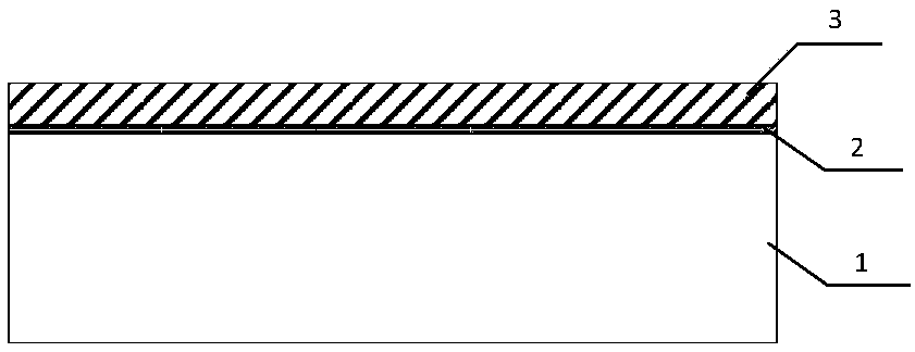
[0047] (1) Choose an N-type silicon wafer with a thickness of 200μm and a crystal orientation of (100) as the silicon-based substrate 1. The silicon-based substrate 1 is washed with propanol, ethanol, and deionized water in sequence, dried with acid The cleaning solution is cleaned, and then soaked in dilute hydrofluoric acid. The acidic cleaning solution is HCl:H with a mass ratio of 1:2:8 2 O 2 :H 2 O's mixed cleaning solution;
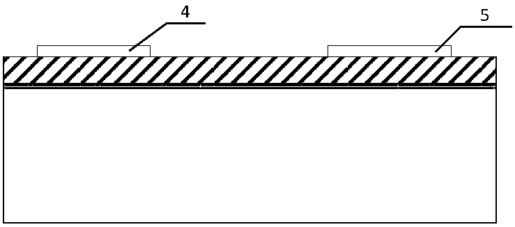
[0048] (2) such as figure 1 with figure 2 As shown, SiO is grown on a silicon substrate 2 Protective layer 2, then in SiO 2 Deposit SiN on the protective layer 2 by LPCVD x Polysilicon layer 3, in SiN x The cantilever beam contact area 4 and the capacitor area 5 are formed on the polysilicon layer 3 by photolithography;
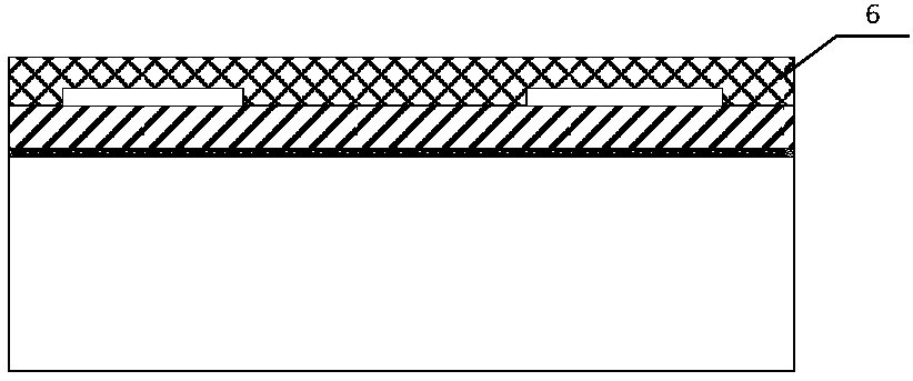
[0049] (3) such a...
Embodiment 2
[0057] In this embodiment, a cantilever beam is taken as an example to specifically describe the MEMS gas sensor in the present invention. The MEMS gas sensor in this embodiment is manufactured by the following steps:
[0058] (1) Choose an N-type silicon wafer with a thickness of 170μm and a crystal orientation of (100) as the silicon-based substrate 1. The silicon-based substrate 1 is washed sequentially with propanol, ethanol, and deionized water, and then dried with acid The cleaning solution is cleaned, and then soaked in dilute hydrofluoric acid. The acidic cleaning solution is HCl:H with a mass ratio of 1:2:8 2 O 2 :H 2 O's mixed cleaning solution;
[0059] (2) such as figure 1 with figure 2 As shown, SiO is grown on a silicon substrate 2 Protective layer 2, then in SiO 2 Deposit SiN on the protective layer 2 by LPCVD x Polysilicon layer 3, in SiN x The cantilever beam contact area 4 and the capacitor area 5 are formed on the polysilicon layer 3 by photolithography;
[0060] ...
Embodiment 3
[0068] In this embodiment, a cantilever beam is taken as an example to specifically describe the MEMS gas sensor in the present invention. The MEMS gas sensor in this embodiment is manufactured by the following steps:
[0069] (1) Choose an N-type silicon wafer with a thickness of 180μm and a crystal orientation of (100) as the silicon-based substrate 1. The silicon-based substrate 1 is washed with propanol, ethanol, and deionized water in sequence, dried by acid The cleaning solution is cleaned, and then soaked in dilute hydrofluoric acid. The acidic cleaning solution is HCl:H with a mass ratio of 1:2:8 2 O 2 :H 2 O's mixed cleaning solution;
[0070] (2) such as figure 1 with figure 2 As shown, SiO is grown on a silicon substrate 2 Protective layer 2, then in SiO 2 Deposit SiN on the protective layer 2 by LPCVD x Polysilicon layer 3, in SiN x The cantilever beam contact area 4 and the capacitor area 5 are formed on the polysilicon layer 3 by photolithography;
[0071] (3) such as ...
PUM
| Property | Measurement | Unit |
|---|---|---|
| thickness | aaaaa | aaaaa |
| thickness | aaaaa | aaaaa |
| thickness | aaaaa | aaaaa |
Abstract
Description
Claims
Application Information
 - R&D
- Intellectual Property
- Life Sciences
- Materials
- Tech Scout
- Unparalleled Data Quality
- Higher Quality Content
- 60% Fewer Hallucinations
Browse by: Latest US Patents, China's latest patents, Technical Efficacy Thesaurus, Application Domain, Technology Topic, Popular Technical Reports.
© 2025 PatSnap. All rights reserved.Legal|Privacy policy|Modern Slavery Act Transparency Statement|Sitemap|About US| Contact US: help@patsnap.com