
Semiconductor device

A semiconductor and device technology, applied in the field of semiconductor devices, can solve the problems of semiconductor device performance degradation, weak ability to withstand negative surge voltage, and limit the use range of semiconductor devices

Active Publication Date: 2018-06-15
SHANGHAI AWINIC TECH CO LTD
View PDF4 Cites 0 Cited by
  • Summary
  • Abstract
  • Description
  • Claims
  • Application Information

AI Technical Summary

Problems solved by technology

[0004] The catastrophic hazards of the surge phenomenon include: the larger surge voltage exceeds the bearing capacity of the semiconductor device, directly burning the semiconductor device; its cumulative hazards include: the cumulative effect of multiple small surges will lead to the decline in the performance of the semiconductor device , which shortens the service life of semiconductor devices
In existing semiconductor devices, the ability to withstand negative surge voltage is weak, which limits the scope of use of semiconductor devices

Method used


Image

  • Semiconductor device
  • Semiconductor device
  • Semiconductor device

Examples


Embodiment Construction

[0031] The following will clearly and completely describe the technical solutions in the embodiments of the present invention with reference to the accompanying drawings in the embodiments of the present invention. Obviously, the described embodiments are only some, not all, embodiments of the present invention. Based on the embodiments of the present invention, all other embodiments obtained by persons of ordinary skill in the art without making creative efforts belong to the protection scope of the present invention.

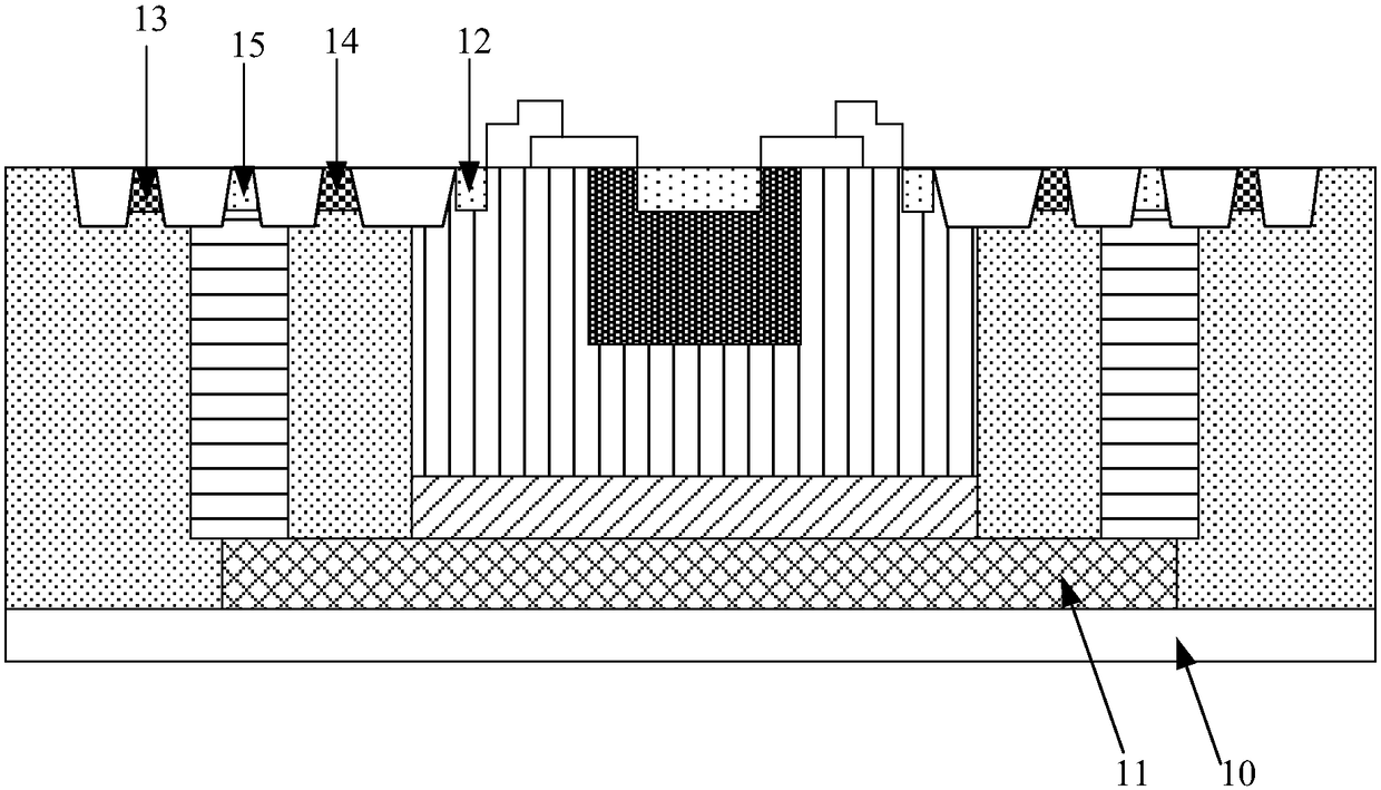
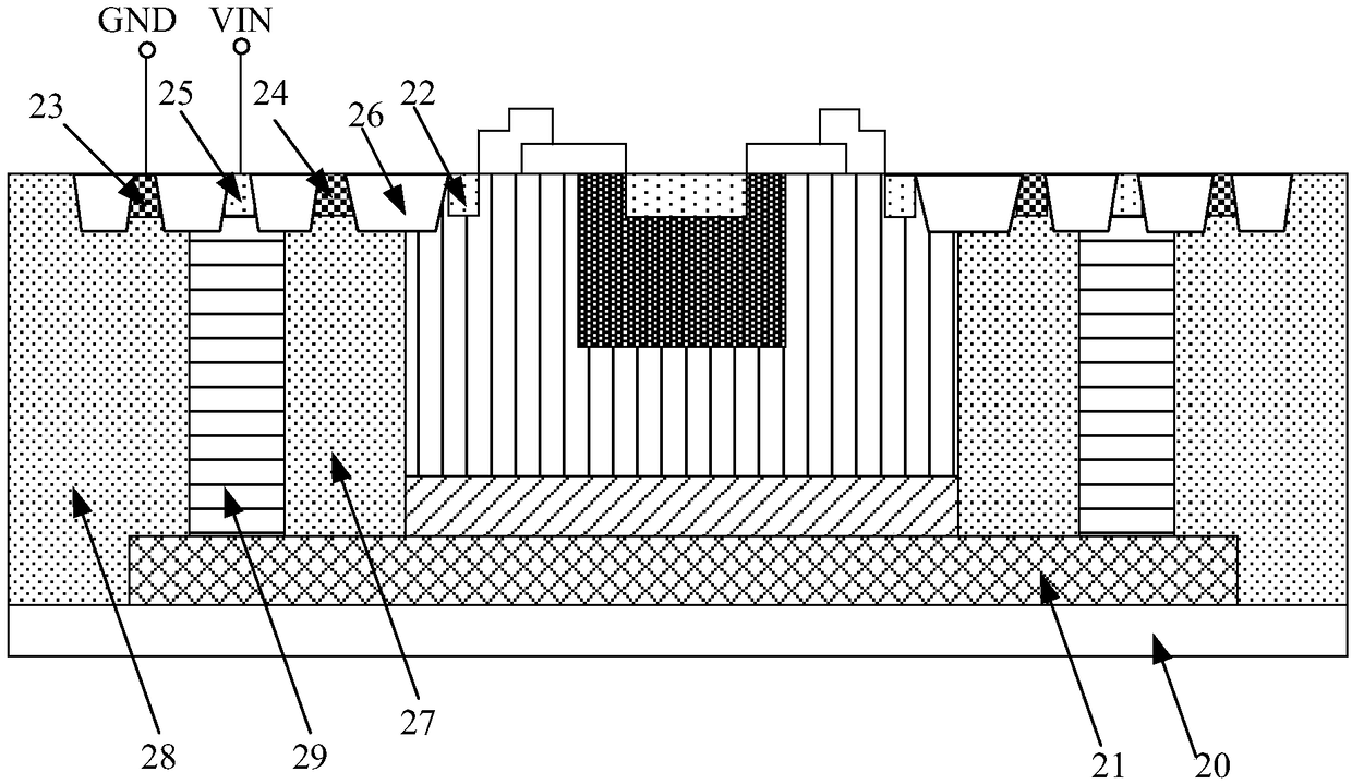
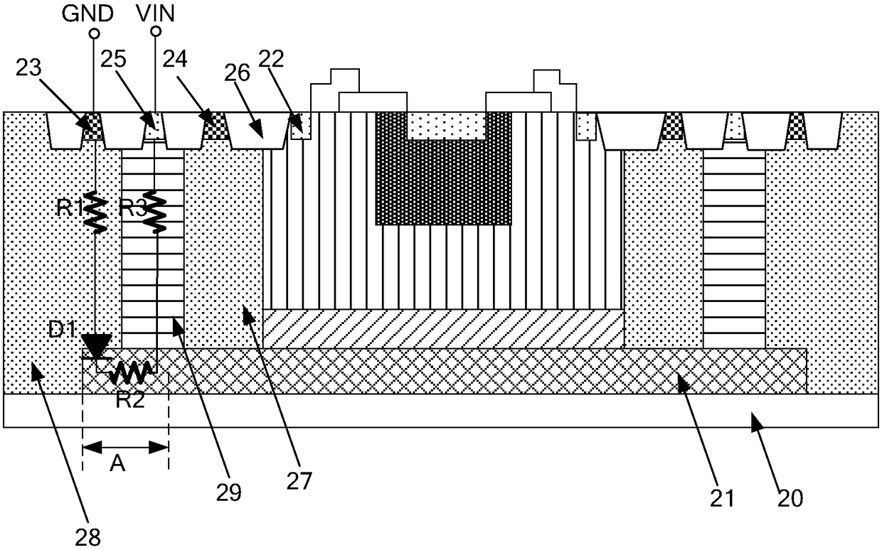
[0032] As mentioned in the background art, the existing semiconductor devices have poor capability of withstanding negative pulse energy, and an LDMOS (lateral double-diffused metal oxide semiconductor, lateral double-diffused metal oxide semiconductor) device is taken as an example below for illustration.

[0033] LDMOS is widely used in various applications due to its balanced characteristics in terms of on-resistance (Rdson) and drain-source breakdown voltag...


PUM


Abstract

The invention discloses a semiconductor device. According to the semiconductor device, the doping concentration of an N-type buried layer is greater than that of a P-type doped region because of the fact that the orthographic projection of the external edge of the N-type buried layer on a P-type substrate covers the orthographic projection of the internal edge of a second P-type ring on the P-typesubstrate in the loop between a second N-type ring and the second P-type ring when the negative voltage pulse is inputted to the second N-type ring so that the resistance in the equivalent circuit can be reduced, more power is enabled to be allocated to the parasitic diode, the characteristic that the parasitic diode can bear high power is utilized and thus the input end of the semiconductor device is enabled to bear high negative surge voltage.

Description

technical field [0001] The present invention relates to the technical field of semiconductors, and more specifically, to a semiconductor device. Background technique [0002] With the continuous development of science and technology, more and more electronic devices are widely used in people's daily life and work, which brings great convenience to people's daily life and work, and has become an indispensable and important tool for people today. tool. [0003] The main control center of electronic equipment to realize various functions is the integrated circuit, and various types of semiconductor devices are important units that constitute the integrated circuit. Surge phenomena are prone to occur in integrated circuits, and instantaneous overvoltages exceeding the normal operating voltage of devices are generated, that is, large surge voltages are generated. The characteristic of the surge phenomenon is that it occurs for a very short time, usually in the order of microsec...

Claims


Application Information

Patent Timeline
IPC IPC(8): H01L29/78
CPCH01L29/7818H01L29/7823
Inventor 程剑涛胡建伟罗旭程
Owner SHANGHAI AWINIC TECH CO LTD
Features
  • Generate Ideas
  • Intellectual Property
  • Life Sciences
  • Materials
  • Tech Scout
  • Unparalleled Data Quality
  • Higher Quality Content
  • 60% Fewer Hallucinations
Learn More