

Starting circuit
A technology for starting circuits and driving circuits, which is applied to electrical components, high-efficiency power electronic conversion, and output power conversion devices, etc., can solve the problem that the boost circuit or the post-stage control circuit cannot be started, and limit the starting voltage of the second-stage boost circuit. , Unable to meet the starting voltage range and other problems, to achieve the effect of meeting the input voltage range, reducing loss, and low loss
- Summary
- Abstract
- Description
- Claims
- Application Information
AI Technical Summary
Problems solved by technology
Method used
Image

Examples
no. 1 example
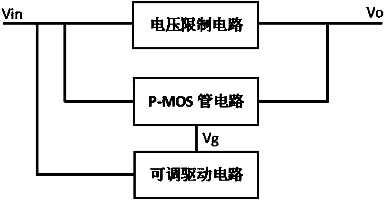
[0037] A startup circuit of the present invention includes a P-MOS transistor TR1, an adjustable drive circuit and a voltage limiting circuit. For each circuit module, combined with the attached Figure 5 The following specific circuits are used to describe the above three features in detail as follows:
[0038] The adjustable driving circuit of the present invention includes a first resistor R1, a second resistor R2, a third resistor R3, a fourth resistor R4, a fifth resistor R5, a sixth resistor R6, a first NPN transistor Q3, and a first PNP transistor Q2. The third resistor R3 is connected between the input voltage Vin and the collector of the first NPN transistor Q3; the fifth resistor R5 is connected between the input voltage Vin and the sixth resistor R6; the other end of the sixth resistor R6 is grounded; The emitter of an NPN transistor Q3 is connected to one end of the fourth resistor R4, and the base is connected to the connection point of the fifth resistor R5 and ...
no. 2 example
[0049] On the basis of the first embodiment, the second embodiment of the present invention can be obtained by modifying the voltage limiting circuit. Figure 5 The specific circuit of the second embodiment is specifically described as follows for the above three features:
[0050] The adjustable driving circuit and the PNP triode circuit described in the present invention are consistent with the first embodiment.
[0051] The difference from the first embodiment is that the voltage limiting circuit of the present invention is a voltage stabilizing circuit, including the second chip IC2. The second chip IC2 can be any chip that has the function of stabilizing the input voltage to output a fixed voltage value. The input end of the second chip IC2 is connected to the input voltage Vin, the ground end of the second chip IC2 is grounded, and the output end of the second chip IC2 is connected to the drain of the P-MOS transistor TR1 as the output voltage Vo of the start-up circuit...
no. 3 example
[0056] On the basis of the first embodiment and the second embodiment, the third embodiment of the present invention can be obtained by improving the voltage limiting circuit, which is attached below Figure 6 The voltage limiting circuit of the third embodiment is described as follows:
[0057] The voltage limiting circuit in this embodiment is also a voltage stabilizing circuit, including the seventh resistor R7, the eighth resistor R8, the second NPN transistor Q4, the first capacitor C1 and the first diode Z1, the first diode Z1 can be 10V regulator tube. One end of the seventh resistor R7 is connected to the collector of the second NPN transistor Q4, and the other end is connected to Vin; one end of the eighth resistor R8 is connected to Vin, and the other end is connected to the base of the second NPN transistor Q4; the first capacitor C1 One end is connected to the base of the second NPN transistor Q4, and the other end is connected to the input ground; the cathode of ...
PUM
 Abstract
Description
Claims
Application Information