
Fluorescence collection and analysis method for array type microfluidic chip

A collection analysis and chip technology, which is applied in the field of micro-full analysis, can solve the problems of limited selection of fluorescent materials, inability of CCD to obtain clear images, and inability to collect pictures accurately and clearly, so as to avoid cumbersome steps and time consumption, and solve the problem of fluorescence Information detection problem, effect of preserving original properties

Active Publication Date: 2018-06-19
NORTHWESTERN POLYTECHNICAL UNIV
View PDF11 Cites 2 Cited by
  • Summary
  • Abstract
  • Description
  • Claims
  • Application Information

AI Technical Summary

Problems solved by technology

The instrument uses laser light to obtain fluorescence information, and the laser wavelength has a certain range, which will inevitably limit the selection of fluorescent materials; for some experiments that require the shortest time to obtain the reaction results after some biological reactions, the instrument will also be delayed in time, which may be lost. Important information after the reaction; and the micro-reaction chamber of some high-density microfluidic chips may be too small, and it is impossible to obtain clear images using only CCD
[0004] The patent with the application number 201710789184.8 proposes a new automatic fluorescence signal acquisition and analysis method based on dPCR. The patent collects images in different regions of the dPCR chip, automatically recognizes the splicing and counts the fluorescence intensity, and realizes full automation. However, the acquisition It takes a long time to make the theoretical position coincide with the actual position in each step of the picture process; when automatically identifying and splicing, the method of first row and second column is adopted to separate the pictures between rows; when extracting the fluorescence intensity, first according to the design size Create the same matrix, and then extract the data of the corresponding position on the photo according to the one-to-one correspondence
This method solves the fluorescence detection of some microfluidic chips to a certain extent, but for the fluorescence detection of some microfluidic chips, there is a problem that the pictures cannot be collected accurately and clearly; and when the divided area increases, the system moves and misplaces, which will cause some problems when splicing. A certain error occurs

Method used


Image

  • Fluorescence collection and analysis method for array type microfluidic chip
  • Fluorescence collection and analysis method for array type microfluidic chip
  • Fluorescence collection and analysis method for array type microfluidic chip

Examples


Embodiment Construction

[0025] The present invention will be described in further detail below in conjunction with the accompanying drawings.

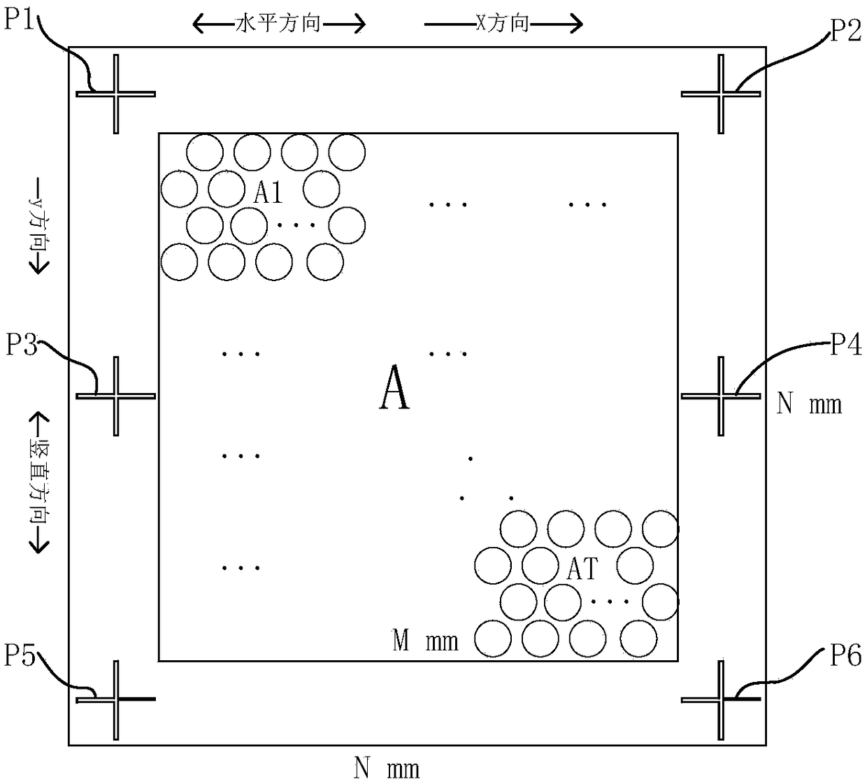
[0026] An array microfluidic chip (the density of the micro-reaction chamber of the chip reaches 570,000 / cm 2 Above) the steps of the fluorescent collection and analysis method are as follows:

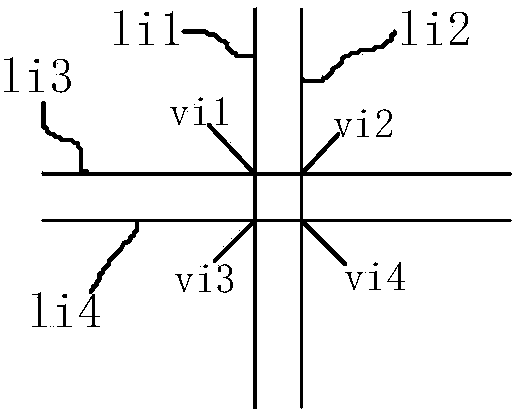
[0027]Step 1: Fabrication of the array microfluidic chip. The array microfluidic chip is a microwell chip with special marks produced by us using micro-nano processing technology, refer to Figure 5 , its overall size is 9.1*9.1㎜, the area A is part of the micro-reaction chamber, the edge size is 8380*8380μm, and the area A is divided into six blocks, which are respectively represented by A1, A2, A3, A4, A5, and A6, six blocks The size of the Ai structure (size is 2766*4194) is exactly the same, and the interval between two adjacent pieces is 21μm. There are six special cross marks in the ring area formed by the edge of the chip and the edge of the micro-reaction ch...


PUM


Abstract

The invention discloses fluorescence collection and analysis method for an array type microfluidic chip and belongs to the technical field of micro total analysis. According to the method, a deflection angle of a whole chip can be calculated by cross marks on the edge of the chip, and corresponding rotation operation can be performed according to the calculated angle during post processing of eachpicture, so that tedious steps and time consumption caused by manual operational measurement are avoided; reaction microchamber parts are easy to distinguish according to intervals, and with adoptionof a partitioned image collection and analysis method, errors caused by splicing and other factors are avoided and original nature of each image is reserved; the problem about fluorescence information detection of the array type microfluidic chip biological reaction is solved, and a foundation is laid for a rapid digital microfluid diagnosis system.

Description

technical field [0001] The invention belongs to the technical field of micro-total analysis, in particular to a fluorescence collection and analysis method of an array microfluidic chip. Background technique [0002] Nowadays, the fluorescence conversion of biological information has become an important method in the field of life science research, and the application of microfluidic chips in biological research is becoming more and more extensive. Functions are transferred to portable analysis devices, such as various chips. In the microfluidic chip analysis system, samples are placed on integrated chips of several square centimeters to achieve high-throughput and low-cost chemical analysis. [0003] The patent No. CN1548944A introduces a microfluidic chip laser-induced fluorescence analyzer. The pinhole of the instrument is equipped with a replaceable CCD camera. It communicates with a computer to obtain image signals. The computer controls the stepping motor and can be se...

Claims


Application Information

Patent Timeline
Patent Type & Authority Applications(China)
IPC IPC(8): G01N35/00
CPCG01N35/00
Inventor 李桦楠帕维尔·诺伊茨尔徐颖张浩卿
Owner NORTHWESTERN POLYTECHNICAL UNIV
Learn More