Organic semiconductor based one-dimensional photonic crystal edge emission laser and implementation method

An edge-emitting laser and organic semiconductor technology, applied in the field of lasers, can solve problems such as unfavorable flat panel all-optical integration, and achieve the effects of reducing production costs and condition requirements, lowering thresholds, and suppressing mode competition.

Active Publication Date: 2018-06-22
MINZU UNIVERSITY OF CHINA
View PDF5 Cites 5 Cited by
  • Summary
  • Abstract
  • Description
  • Claims
  • Application Information

AI Technical Summary

Problems solved by technology

[0008] (3) Research work on organic semiconductors DBR, DFB, DBR-DFB, photonic crystal quasicrystals, and band-edge emitting lasers is mainly based on surface emission, which is not conducive to future flat-panel all-optical integration;

Method used


Image

  • Organic semiconductor based one-dimensional photonic crystal edge emission laser and implementation method
  • Organic semiconductor based one-dimensional photonic crystal edge emission laser and implementation method
  • Organic semiconductor based one-dimensional photonic crystal edge emission laser and implementation method

Examples


Embodiment Construction

[0044] The present invention will be further elaborated below through specific embodiments in conjunction with the accompanying drawings.

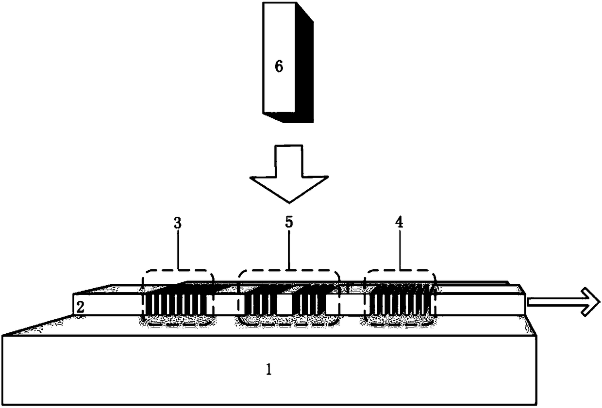
[0045] Such as figure 1 As shown, the one-dimensional photonic crystal edge-emitting laser based on organic semiconductors of the present embodiment includes: a substrate 1, a gain medium 2, a total reflection structure 3, a partial transmission structure 4, a mode selection structure 5 and a pump source 6; wherein, in The upper surface of the substrate 1 is spin-coated with an organic semiconductor luminescent material, the refractive index of the substrate is lower than that of the organic semiconductor luminescent material; the organic semiconductor luminescent material is etched to form a ridge-shaped gain medium 2 on the substrate as a ridge-shaped waveguide; Three photonic crystal gratings parallel to each other are respectively formed on the gain medium 2, and the photonic crystal gratings are perpendicular to the surface of the sub...


PUM


Abstract

The invention discloses an organic semiconductor based one-dimensional photonic crystal edge emission laser and an implementation method. The laser uses a ridge-shaped gain medium formed on a substrate as a ridge-shaped waveguide, three photonic crystal gratings formed by one-dimensional photonic crystals are formed on the gain medium, the photonic crystal gratings at two sides are resonant cavities are of an all-trans structure or a partial transmission structure respectively and form a resonant cavity; and the photonic crystal grating between the photonic crystal gratings at the two sides isof a mode selection structure, and can only allow transmission of light near a target wavelength. The manufacturing cost and the condition demand of a laser are greatly reduced and lowered; the problem that an cleavage plane of an inorganic crystal material cannot be used as an outgoing window of an edge emission laser can be solved, and a good laser outgoing window can be manufactured easily; aflat plate all-optical integrated device can be easily integrated; a threshold is lowered, mode competition is suppressed, and an interface mode is effectively suppressed; and an edge emission organiclaser which is low in cost, is easy to process, is long in gain, is low in threshold, and is easy to integrate is realized.

Description

technical field [0001] The invention relates to a laser, in particular to an organic semiconductor-based one-dimensional photonic crystal edge-emitting laser and a realization method. Background technique [0002] Lasers, atomic energy, computers and semiconductors are called the "New Four Great Inventions" of the 20th century. With the advancement of material science and process technology, the development and application of various new semiconductor lasers have made rapid progress, and are widely used in many fields such as information, industry, medical treatment and national defense. [0003] Throughout the development process of inorganic semiconductor lasers with various wavelengths, high-quality inorganic semiconductor materials are the key to the preparation of high-performance lasers. At present, the methods used by various research teams to prepare the core materials of semiconductor lasers are mainly molecular beam epitaxy and metal-organic vapor phase epitaxy. ...

Claims


Application Information

Patent Timeline
Patent Type & Authority Applications(China)
IPC IPC(8): H01S5/22H01S5/10H01S5/04H01S5/36
CPCH01S5/041H01S5/22H01S5/36H01S5/11
Inventor 陈笑李长伟王义全蔡园园王晓青
Owner MINZU UNIVERSITY OF CHINA
Why Eureka
Try Eureka