

Micro-lens array capable of reducing optical crosstalk between pixels of polarization imaging device
A technology of microlens array and polarization imaging, which is applied in the field of microlens array, can solve the problems of optical crosstalk and entering adjacent pixels, and achieve the effect of reducing optical crosstalk
- Summary
- Abstract
- Description
- Claims
- Application Information
AI Technical Summary
Problems solved by technology
Method used
Image

Examples
Embodiment
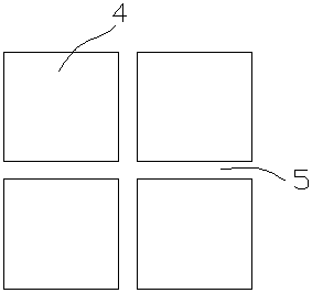
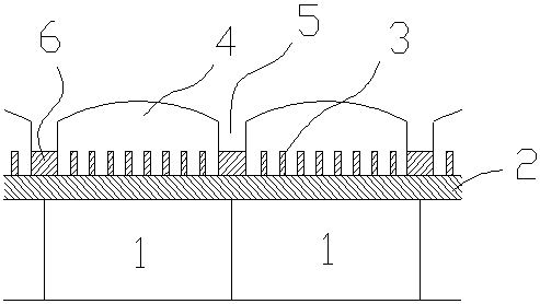
[0020] Prepare a CCD chip with a pixel size of 7.4 μm; deposit a silicon dioxide film on the CCD chip, and process the silicon dioxide film by chemical or mechanical polishing to obtain a planarization layer 2; deposit 200 nm of aluminum on the surface of the planarization layer 2 The aluminum layer is etched into a grating array by using an electron beam lithography process. In the grating array, a single subwavelength grating 3 has a line width of 140nm, a period of 300nm, and a frame width of 340nm; A layer of polymethyl methacrylate is heated and cured; the polymethyl methacrylate is etched into an array corresponding to the pixel by mask photolithography; the polymethyl methacrylate is melted by heating to obtain a microlens array ; Use photolithography to etch an isolation groove 5 with a width of 800 nm between adjacent microlenses 4 . In the prior art, when the microlens array is not installed, the optical crosstalk between the pixels of the polarization imaging device...
PUM
 Abstract
Description
Claims
Application Information