Method for etching super-conduction quantum chip containing niobium film

A superconducting quantum and chip technology, which is applied in the manufacture/processing of superconductor devices, etc., can solve the problems of rough film edges, dotted residues, and difficulty in removal, so as to reduce etching time, smooth film edges, and save etching time Effect

Active Publication Date: 2018-06-29
ORIGIN QUANTUM COMPUTING TECH (HEFEI) CO LTD
View PDF3 Cites 2 Cited by
  • Summary
  • Abstract
  • Description
  • Claims
  • Application Information

AI Technical Summary

Problems solved by technology

[0005] Aiming at the problem of over-etching and serious substrate damage in the existing quantum chip niobium film etching process when the etching time is fast, and the problem that the edge of the film is rough and dotted and difficult to remove when the etching time is slow, the present invention Provided is a superconducting quantum chip etching method containing niobium film

Method used


Image

  • Method for etching super-conduction quantum chip containing niobium film
  • Method for etching super-conduction quantum chip containing niobium film
  • Method for etching super-conduction quantum chip containing niobium film

Examples


Embodiment 1

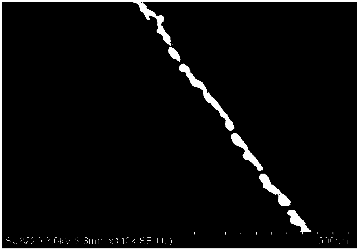
[0052] Using a high-density plasma etching machine for post-processing, the obtained superconducting quantum chip containing niobium film, the etching method is as follows:

[0053] (1) Substrate cleaning: select high-purity silicon wafers as the substrate of the chip. The substrate is the substrate, and the substrate is cleaned with 1-methyl-2-pyrrolidone solution at room temperature for 3 minutes, then transferred to isopropanol at 20°C for 3 minutes, and then in deionized water at 20°C for 3 minutes, then taken out and dried , and then put into a mixed solution composed of concentrated sulfuric acid and 30% mass concentration of hydrogen peroxide, the volume ratio of the concentrated sulfuric acid and the 30% mass concentration of hydrogen peroxide is 7:3, heated to 100°C, soaked for 5min, and then Rinse it with deionized water, dry it with nitrogen, put it into the BOE solution, soak for 3 minutes, take it out, rinse it with deionized water and blow it dry with nitrogen. T...

Embodiment 2

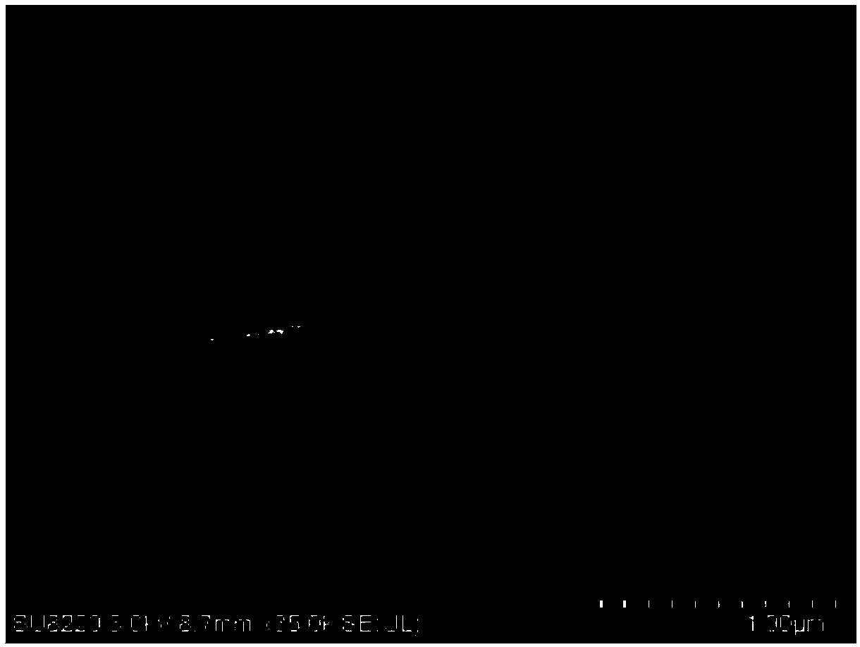
[0064] Using a high-density plasma etching machine for post-processing, the obtained superconducting quantum chip containing niobium film, the etching method is as follows:

[0065] (1) Substrate cleaning: select high-purity silicon wafers as the substrate of the chip. The substrate is the substrate, and the substrate is cleaned with 1-methyl-2-pyrrolidone solution at room temperature for 9 minutes, then transferred to isopropanol at 25°C for 12 minutes, and then in deionized water at 25°C for 12 minutes, taken out and dried , and then put into a mixed solution composed of concentrated sulfuric acid and 30% mass concentration of hydrogen peroxide, the volume ratio of the concentrated sulfuric acid and the 30% mass concentration of hydrogen peroxide is 7:3, heated to 115 ° C, soaked for 12min, and then used Rinse with deionized water, dry with nitrogen, put in BOE solution, soak for 4min, take out, rinse with deionized water and blow dry with nitrogen. The BOE solution consists...

Embodiment 3

[0076] Using a high-density plasma etching machine for post-processing, the obtained superconducting quantum chip containing niobium film, the etching method is as follows:

[0077] (1) Substrate cleaning: select high-purity silicon wafers as the substrate of the chip. The substrate is the substrate, and the substrate is cleaned with 1-methyl-2-pyrrolidone solution at room temperature for 15 minutes, then transferred to isopropanol at 30°C for 15 minutes, and then in deionized water for 15 minutes at 30°C, then taken out and dried , and then put into a mixed solution composed of concentrated sulfuric acid and 30% mass concentration of hydrogen peroxide, the volume ratio of the concentrated sulfuric acid and the 30% mass concentration of hydrogen peroxide is 7:3, heated to 130 ° C, soaked for 20min, and then used Rinse with deionized water, dry with nitrogen, and finally put in BOE solution, soak for 5 minutes, take it out, rinse with deionized water, and dry with nitrogen. The...


PUM


Abstract

The invention discloses a method for etching a super-conduction quantum chip containing a niobium film, belongs to the field of super-conduction quantum chips, and aims to solve the problems of over-etching due to high etching speed, severe damage of a substrate, rough edge of a film even if the etching speed is low, and difficulty in removing dotted residues in the existing quantum chip niobium film etching process are solved. The method comprises the following steps: (1) cleaning the substrate to obtain a clean substrate; (2) plating the substrate with the niobium film to obtain a substrateplated with the niobium film; (3) exposing and developing the niobium film on the substrate plated with the niobium film to obtain a developed substrate; (4) etching the substrate; (5) performing post-treatment on the etched substrate to obtain a post-treated substrate; and removing glue from the post-treated substrate. By adopting the method, the niobium film can be rapidly etched, simultaneously, the dotted residues can be removed effectively, over-etching is avoided, and the effects of clean etching surface and flat graphic edge are achieved.

Description

technical field [0001] The invention belongs to the technical field of integrated circuit micro-nano processing, and in particular relates to an etching method for a superconducting quantum chip containing a niobium film. Background technique [0002] Micro-nano processing technology is widely used in the fabrication of integrated circuits. The steps of general integrated circuit manufacturing are: first, deposit a layer of film on the substrate by means of sputtering evaporation, etc., and then coat a layer of photoresist composed of photosensitive substances and solvents. After the photoresist is sensitized, the part of the photosensitive layer that is irradiated or the part that is not irradiated is left on the surface of the base material through development. The remaining photoresist pattern is the designed pattern, and then removed by etching or etching. The parts not covered by the photoresist are removed, and the designed pattern is transferred to the surface of the...

Claims


Application Information

Patent Timeline
Patent Type & Authority Applications(China)
IPC IPC(8): H01L39/24
CPCH10N60/01
Inventor 杨夏朱美珍
Owner ORIGIN QUANTUM COMPUTING TECH (HEFEI) CO LTD
Why Eureka
Try Eureka