
TFT substrate and manufacturing method thereof

A manufacturing method and substrate technology, which is applied in semiconductor/solid-state device manufacturing, instruments, semiconductor devices, etc., can solve problems such as difficult control of parameters, peeling of protective layer, poor display of liquid crystal panels, etc., to reduce undercut phenomenon and tilt angle Small, well-displayed effects

Active Publication Date: 2020-09-29
WUHAN CHINA STAR OPTOELECTRONICS TECH CO LTD
View PDF3 Cites 2 Cited by
  • Summary
  • Abstract
  • Description
  • Claims
  • Application Information

AI Technical Summary

Problems solved by technology

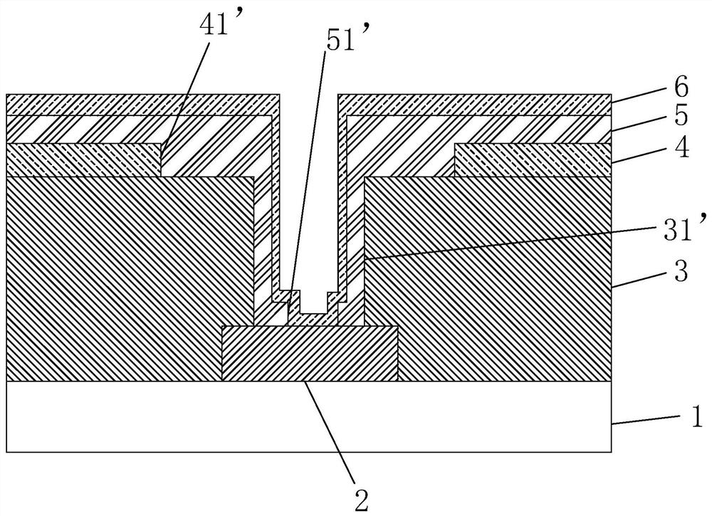
Since the parameters of the manufacturing process of the TFT substrate are not easy to control, the bottom common electrode 4 often has an undercut phenomenon at the second via hole 41 ′, causing the bottom common electrode 4 to be close to the edge of the second via hole 41 ′. warping, which in turn leads to the phenomenon of peeling (peeling) of the protective layer 5 disposed on the bottom common electrode 4, resulting in poor display of the liquid crystal panel

Method used


Image

  • TFT substrate and manufacturing method thereof
  • TFT substrate and manufacturing method thereof
  • TFT substrate and manufacturing method thereof

Examples


Embodiment Construction

[0031] In order to further illustrate the technical means adopted by the present invention and its effects, the following describes in detail in conjunction with preferred embodiments of the present invention and accompanying drawings.

[0032] The drawings in this application are only schematic diagrams. Unless otherwise specified, they do not mean that the actual thickness ratio, flatness, and shape of each film layer are the same as those in the drawings. There are some differences from the schematic diagram, for example, the shape of the hole and the appearance of the combined part of each film layer will be different from the schematic diagram, which can be understood and known by those skilled in the art. The description of the sequence of process steps and the structure of the film layer in this application only indicates the sequence and relative position of the steps and film layers directly related to the technical problems of this application, and does not mean that ...


PUM

PropertyMeasurementUnit
lengthaaaaaaaaaa
transmittivityaaaaaaaaaa

Abstract

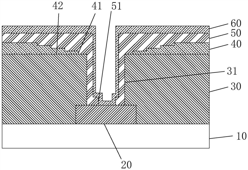
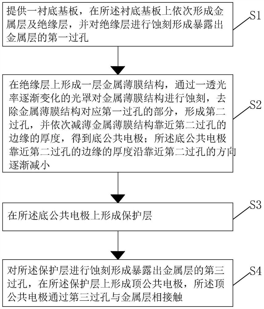
The invention provides a TFT substrate and a manufacturing method thereof. The TFT substrate comprises a base substrate, a metal layer arranged on the base substrate, an insulating layer arranged on the base substrate and the metal layer, a bottom common electrode arranged on the insulating layer, and a protective layer arranged on the insulating layer and the bottom common electrode. The insulating layer has first via holes exposing the metal layer. The bottom common electrode has second via holes formed in areas corresponding to the first via holes. The thickness of the edge of the bottom common electrode near the second via holes gradually decreases along the direction near the second via holes, so that the upwarp angle of the edge of the bottom common electrode near the second via holes is reduced, and the probability of bottom cutting is reduced. Therefore, the risk of peeling of the film formed on the bottom common electrode is reduced, the yield of the TFT substrate is improved,and the display effect of the LCD panel is good.

Description

technical field [0001] The invention relates to the field of display technology, in particular to a TFT substrate and a manufacturing method thereof. Background technique [0002] With the development of display technology, liquid crystal displays (Liquid Crystal Display, LCD) and other flat display devices are widely used in mobile phones, televisions, personal Various consumer electronic products such as digital assistants, digital cameras, notebook computers, and desktop computers have become the mainstream of display devices. [0003] Most of the liquid crystal displays currently on the market are backlight liquid crystal displays, which include a liquid crystal display panel and a backlight module. The working principle of the liquid crystal display panel is to pour liquid crystal molecules between the thin film transistor array substrate (ThinFilm Transistor Array Substrate, TFT Array Substrate) and the color filter substrate (ColorFilter Substrate, CF Substrate), and...

Claims


Application Information

Patent Timeline
Patent Type & Authority Patents(China)
IPC IPC(8): H01L27/12H01L21/84G02F1/1362
CPCG02F1/136227H01L27/1244H01L27/1259
Inventor 高玲
Owner WUHAN CHINA STAR OPTOELECTRONICS TECH CO LTD
Learn More