

CZTS laminated absorption layer based on magnetron sputtering method and preparation method thereof
A technology of magnetron sputtering and absorption layer, which is applied in the direction of final product manufacturing, sustainable manufacturing/processing, photovoltaic power generation, etc., to achieve the effect of improving efficiency, fast reaction speed, and non-toxic production raw materials
- Summary
- Abstract
- Description
- Claims
- Application Information
AI Technical Summary
Problems solved by technology
Method used
Image

Examples
Embodiment 1
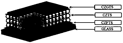
[0048] Embodiment 1: as figure 1 As shown in the schematic diagram of the structure of the CZTS superimposed absorbing layer, the CZTS superimposed absorbing layer in this example is prepared by magnetron sputtering method, from bottom to top is the substrate, Fe-doped Cu 2 ZnSnS 4 Absorber layer, undoped Cu 2 ZnSnS 4 Absorber layer, Cu doped with Ge 2 ZnSnS 4 Absorber layer; Cu doped with Fe 2 ZnSnS 4 The thickness of the absorbing layer is 510nm, undoped Cu 2 ZnSnS 4 The thickness of the absorbing layer is 500nm, Ge-doped Cu 2 ZnSnS 4 The thickness of the absorbing layer is 510nm;
[0049] The preparation method of the CZTS laminated absorbing layer in this embodiment, the specific steps are:
[0050] (1) Install the quaternary CZTS semiconductor target, Fe source target, and Ge source target in the magnetron sputtering chamber, and adjust the target base distance between the target and the substrate in the sputtering chamber; the target base distance of the Fe so...
Embodiment 2
[0060] Embodiment 2: as figure 1 As shown in the schematic diagram of the structure of the CZTS superimposed absorbing layer, the CZTS superimposed absorbing layer in this example is prepared by magnetron sputtering method, from bottom to top is the substrate, Fe-doped Cu 2 ZnSnS 4 Absorber layer, undoped Cu 2 ZnSnS 4 Absorber layer, Cu doped with Ge 2 ZnSnS 4 Absorber layer; Cu doped with Fe 2 ZnSnS 4 The thickness of the absorbing layer is 550nm, undoped Cu 2 ZnSnS 4 The thickness of the absorbing layer is 720nm, Ge-doped Cu 2 ZnSnS 4 The thickness of the absorbing layer is 550nm;
[0061] The preparation method of the CZTS laminated absorbing layer in this embodiment, the specific steps are:
[0062] (1) Install the quaternary CZTS semiconductor target, Fe source target, and Ge source target in the magnetron sputtering chamber, and adjust the target base distance between the target and the substrate in the sputtering chamber; the target base distance of the Fe so...
Embodiment 3
[0072] Embodiment 3: as figure 1 As shown in the schematic diagram of the structure of the CZTS superimposed absorbing layer, the CZTS superimposed absorbing layer in this example is prepared by magnetron sputtering method, from bottom to top is the substrate, Fe-doped Cu 2 ZnSnS 4 Absorber layer, undoped Cu 2 ZnSnS 4 Absorber layer, Cu doped with Ge 2 ZnSnS 4 Absorber layer; Cu doped with Fe 2 ZnSnS 4 The thickness of the absorbing layer is 650nm, undoped Cu 2 ZnSnS 4 The thickness of the absorbing layer is 800nm, Cu doped with Ge 2 ZnSnS 4 The thickness of the absorbing layer is 650nm;
[0073] The preparation method of the CZTS laminated absorbing layer in this embodiment, the specific steps are:
[0074] (1) Install the quaternary CZTS semiconductor target, Fe source target, and Ge source target in the magnetron sputtering chamber, and adjust the target base distance between the target and the substrate in the sputtering chamber; the target base distance of the ...
PUM
| Property | Measurement | Unit |
|---|---|---|
| thickness | aaaaa | aaaaa |
| thickness | aaaaa | aaaaa |
| thickness | aaaaa | aaaaa |
Abstract
Description
Claims
Application Information