

Double-row and multiple-row LED lamp baseband
A lamp base and lamp bead technology, which is applied in lighting and heating equipment, semiconductor devices of light-emitting elements, flat light sources, etc., can solve the problems of complex production process, many production steps, and difficult processing, and achieves fewer production processes and fewer lines. Precise layout and less environmental pollution
- Summary
- Abstract
- Description
- Claims
- Application Information
AI Technical Summary
Problems solved by technology
Method used
Image

Examples
Embodiment 1
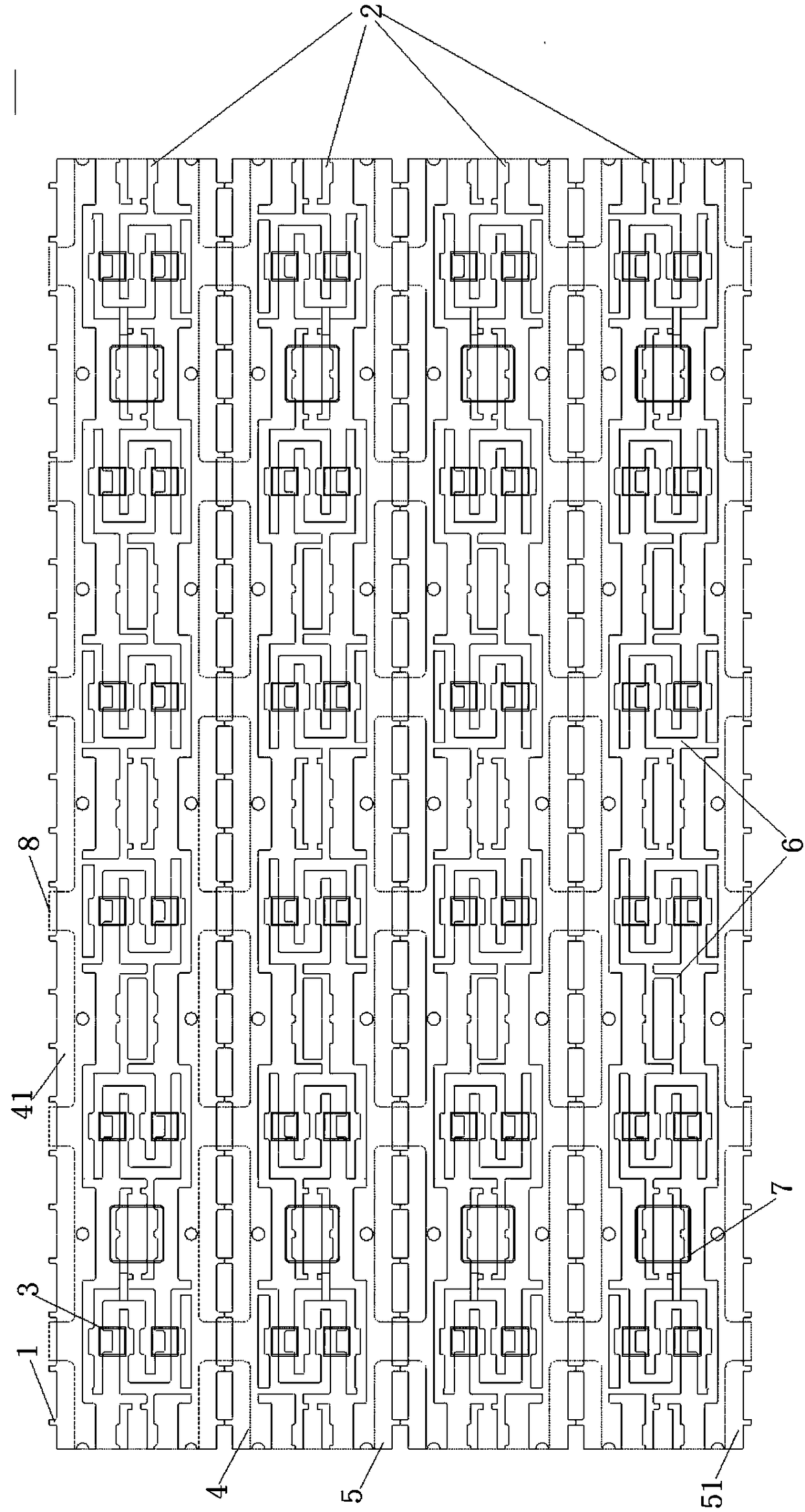
[0020] Such as figure 1 As shown, a double-row, multi-row LED lamp base strip, which includes a circuit base strip 1 and lamp beads 3, the circuit base strip 1 is integrally punched and formed by a bendable conductive metal strip, and multiple lights are formed on the conductive metal strip. A line belt 2 arranged in a parallel direction, the line belt 2 is provided with two first power supply lines 4 and a second power supply line 5 arranged in the parallel direction, and a plurality of lines connected in parallel to the first power supply Component line 6 between line 4 and second power supply line 5 .
[0021] The circuit base belt 1 in the present invention is integrally stamped and formed by a bendable conductive metal strip, the overall circuit layout is accurate and stable, and the production process is less, no printed circuit is needed, waste materials are easy to recycle, less environmental pollution, and easy to realize automatic or semi-automatic production. Autom...
Embodiment 2
[0028] Compared with Embodiment 1, the main difference is that when the output voltages of the first power supply line 4 and the second power supply line 5 are greater than the sum of the rated voltages of the lamp beads 3 of each element line 6 , the The double-row and multi-row LED lamp base strips also include a resistance element 9 mounted on the element line 6 and connected in series with the lamp beads 3 of the same element line 6 . The setting of the resistance element 9 can act as a voltage divider to prevent the actual voltage of the lamp bead 3 from being higher than the rated voltage, thereby damaging the lamp bead 3 and avoiding potential safety hazards caused by long-term use.
[0029] More preferably, the transparent insulating film 8 covers the entire outer surfaces of the element circuit 6 , the lamp bead 3 and the resistance element 9 and part of the outer surfaces of the first power supply circuit 4 and the second power supply circuit 5 . Since there are many...
PUM
| Property | Measurement | Unit |
|---|---|---|
| Thickness | aaaaa | aaaaa |
Abstract
Description
Claims
Application Information