Semiconductor laser material passivation method

A laser and semiconductor technology, applied in the direction of semiconductor lasers, lasers, laser components, etc., can solve problems such as surface residues, poor vacuum environment, surface pollution, etc., reduce surface state density and non-radiative recombination centers, and improve optical performance , to avoid the effect of spreading

Pending Publication Date: 2018-07-17
CHANGCHUN UNIV OF SCI & TECH
View PDF8 Cites 5 Cited by
  • Summary
  • Abstract
  • Description
  • Claims
  • Application Information

AI Technical Summary

Problems solved by technology

[0004] In the existing manufacturing process of semiconductor laser devices, there are usually problems of oxidation, surface residue and surface contamination on the cleavage surface of the Bar bar. The main reason for this problem is the vacuum environment in which the epitaxial wafer is cleaved. Poor, resulting in low damage threshold of the cavity surface of the semiconductor laser, and the cavity surface damage threshold of the semiconductor laser is an important factor affecting the output power and life of the semiconductor laser. Therefore, effective processing of the cavity surface of the semiconductor laser resonator can Effectively increase the laser output power of semiconductor lasers, improve the life of semiconductor lasers and the stability of device performance

Method used


Image

  • Semiconductor laser material passivation method
  • Semiconductor laser material passivation method
  • Semiconductor laser material passivation method

Examples


Embodiment Construction

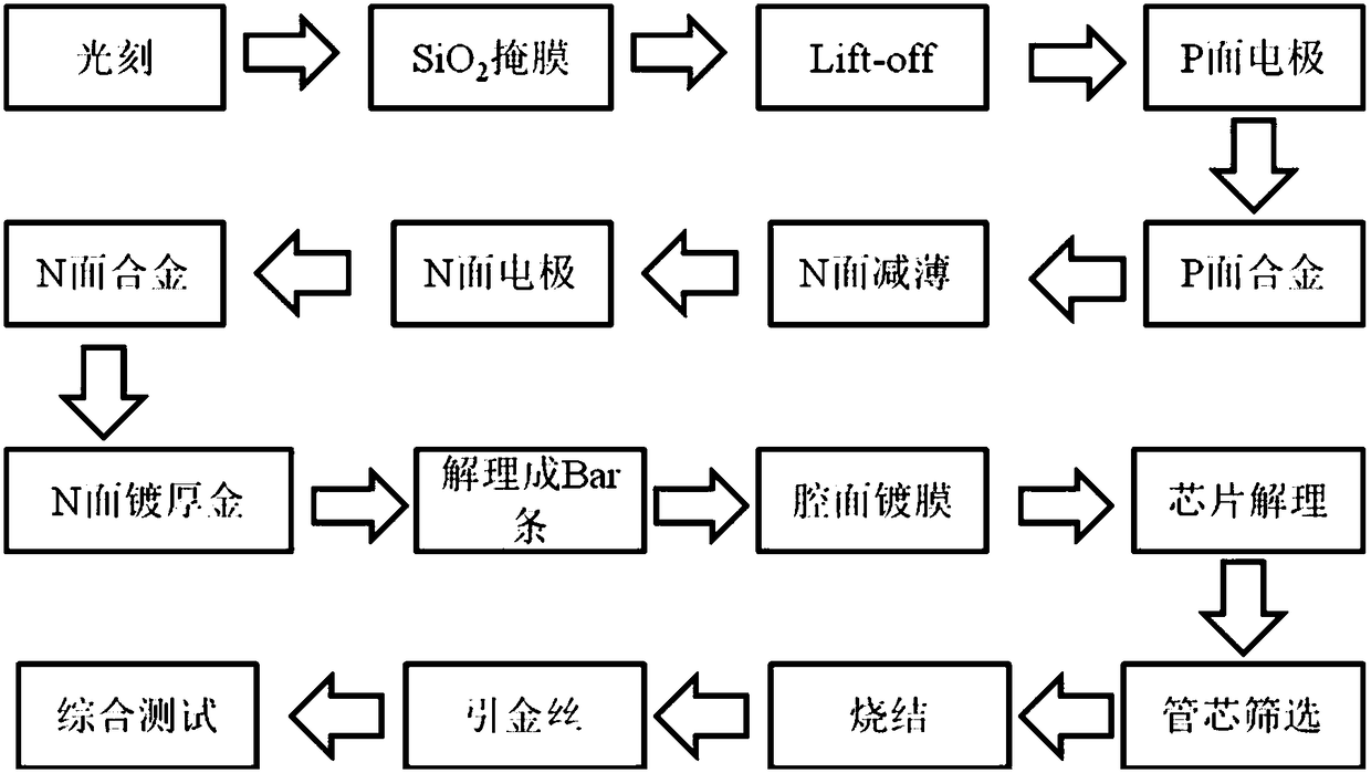
[0012] The following is a further detailed description of the semiconductor laser material passivation method proposed by the present invention, specifically the technical solution for the processing method of the cavity surface material of the semiconductor laser resonator cavity, by using the drawings and specific embodiments.

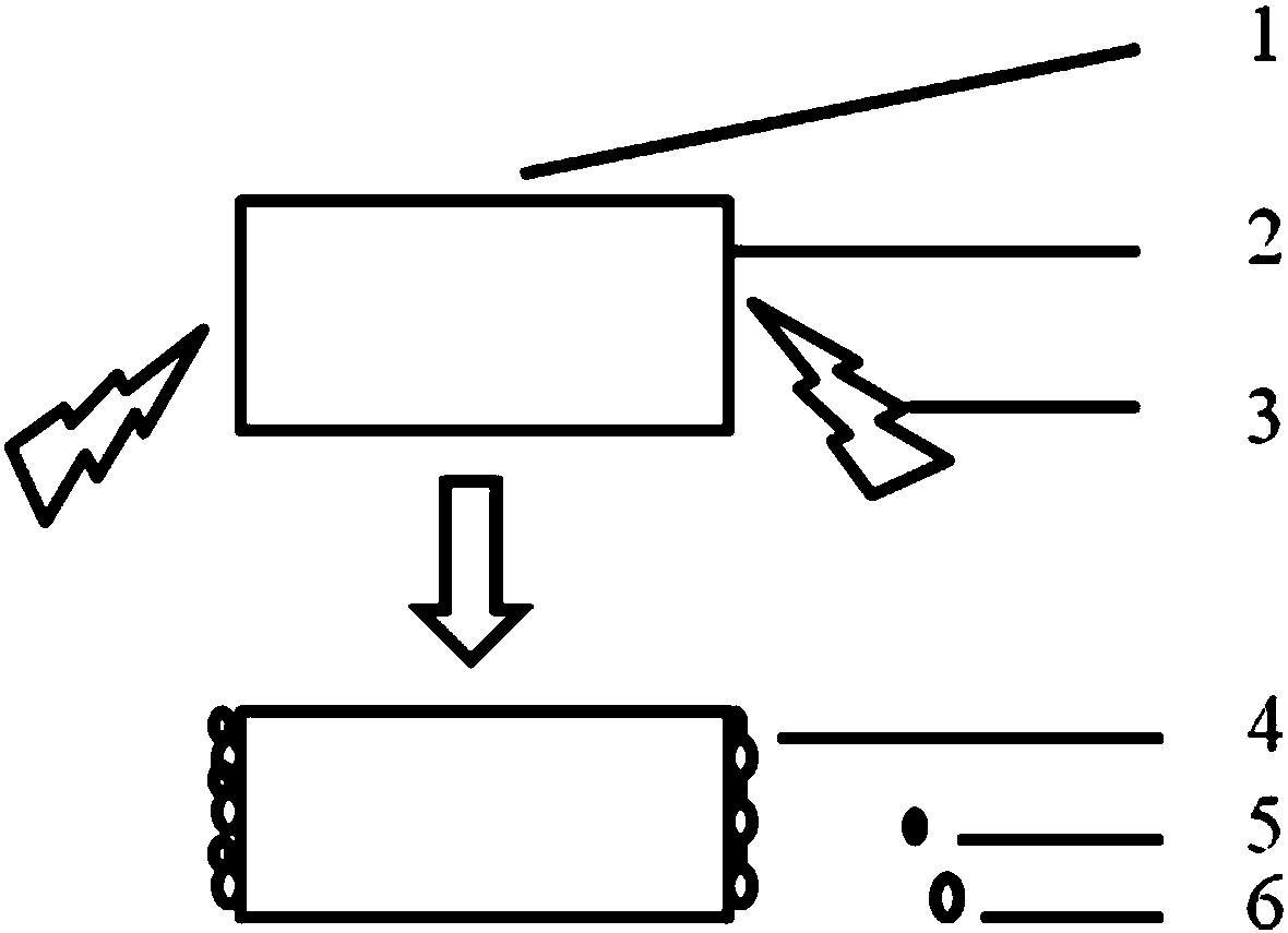
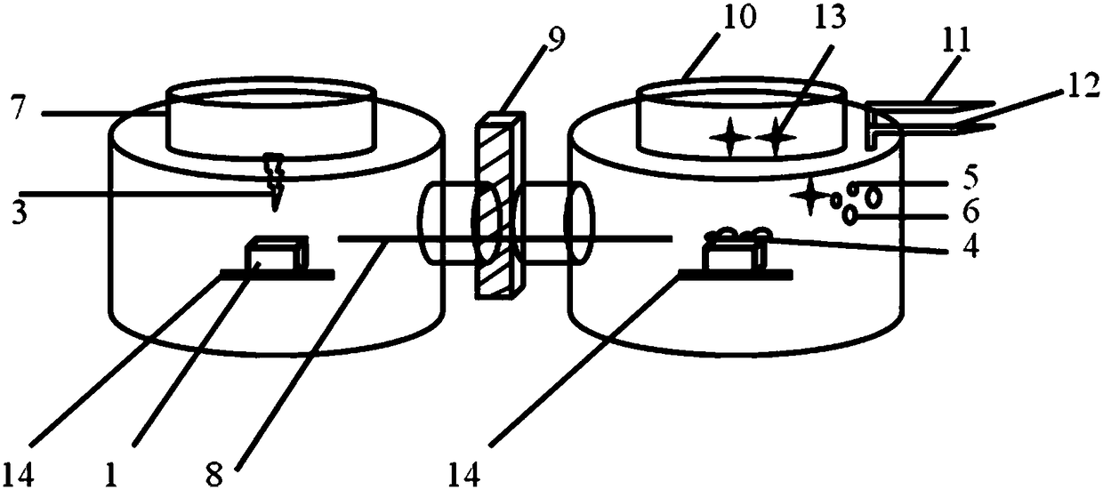
[0013] The present invention proposes a semiconductor laser material passivation method, the method first carries out ion bombardment cleaning to the cavity surface of the semiconductor laser cavity, and then uses ALD technology to deposit a passivation layer on the cavity surface of the cleaned semiconductor laser cavity to improve the efficiency of the semiconductor laser cavity. The cavity surface is protected, and the method mainly includes 3 steps: 1. The semiconductor laser epitaxial wafer is cleaved into Bar strips; 2. The semiconductor laser Bar strips are entered in the semiconductor laser resonator cavity surface processing device proposed by...


PUM


Abstract

The invention discloses a semiconductor laser material passivation method. The method is applicable to passivation treatment of a cavity surface material of a semiconductor laser resonant cavity; themethod specifically comprises the steps of performing bombardment cleaning on the cavity surface material of the semiconductor laser resonant cavity by adopting ion beams, and depositing an AlN passivation layer on the cavity surface of the semiconductor laser resonant cavity by adopting an ALD technology. According to the semiconductor laser material passivation method disclosed in the invention,the surface of the resonant cavity is bombarded by the ion beams in a vacuum environment to effectively remove an oxide layer form the cavity surface, cavity surface pollutants, surface state, surface material dislocation and surface material dangling bond to obtain a clean semiconductor laser resonant cavity surface, and then low-temperature deposition in an ALD apparatus is realized in a plasmaauxiliary condition to obtain the AlN passivation layer for protecting the cavity surface of the resonant cavity. By virtue of the method disclosed in the invention, by performing process treatment on the resonant cavity surface, the cavity surface damage threshold value of the semiconductor laser is improved, and improvement of the output power, the service life and performance stability of thedevice is realized.

Description

technical field [0001] The invention relates to the field of semiconductor lasers, in particular to a semiconductor laser preparation process, in particular to a semiconductor laser resonator cavity surface material surface passivation process, the process combines ion bombardment and atomic layer deposition in the semiconductor laser resonator surface material passivation process The technology is carried out in a vacuum environment, which effectively reduces the surface state density and non-radiative recombination center of the semiconductor laser resonator cavity surface material, and improves the luminous efficiency, laser output power and laser device life of the semiconductor laser device. Background technique [0002] Semiconductor lasers have the advantages of small size, light weight, long life, low cost, and easy mass production. They are widely used in the entire field of optoelectronics and have become the core devices in the field of optoelectronic science today...

Claims


Application Information

Patent Timeline
Patent Type & Authority Applications(China)
IPC IPC(8): H01S5/028
CPCH01S5/0282
Inventor 魏志鹏方铉唐吉龙贾慧民房丹李浩林李如雪郝永琴王晓华马晓辉
Owner CHANGCHUN UNIV OF SCI & TECH
Why Eureka
Try Eureka