Positron emission computer tomography detector device
A technology of positron emission and tomography, which is applied in radiation detection devices, instruments for radiological diagnosis, diagnosis, etc., can solve problems such as inaccurate detection of photon receiving time and attenuation of high-frequency parts
- Summary
- Abstract
- Description
- Claims
- Application Information
AI Technical Summary
Problems solved by technology
Method used
Image

Examples
Embodiment 1
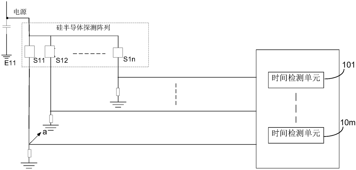
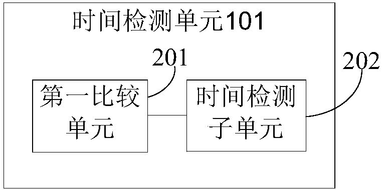
[0066] The positron emission computed tomography detector device provided in this embodiment may include: a silicon semiconductor detection array, and the silicon semiconductor detection array may include a plurality of silicon semiconductor detection units. Wherein, each cathode of the plurality of silicon semiconductor detection units can be connected to a power supply; each anode of the plurality of silicon semiconductor detection units can be respectively used as a first signal output terminal and connected to a corresponding time detection circuit, and the time detection circuit It can be used to detect the receiving time of photons, and the number of the time detection circuit is more than one and less than or equal to the number of the first signal output terminals.
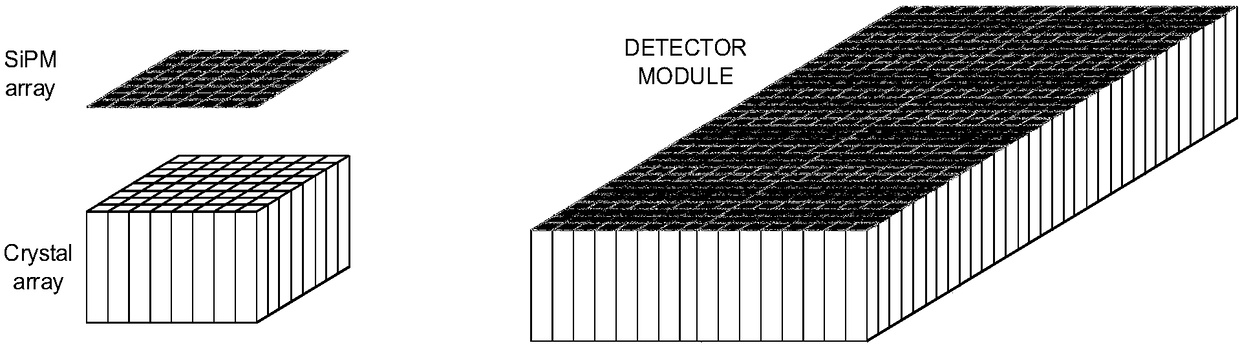
[0067] It should be noted that the silicon semiconductor detection array can be coupled with the scintillation crystal array, for example, the silicon semiconductor detection array can be coupled with the s...
Embodiment 2
[0083] This embodiment provides a positron emission computed tomography detector device. Based on the device embodiment 1, each first signal output terminal of a plurality of silicon semiconductor detection units can also be connected to a one-to-one corresponding crystal position identification circuit, The crystal position identification circuit can be used to identify the position of a scintillation crystal hit by a gamma photon.
[0084] Next, continue to take the silicon semiconductor detection unit S11 in the first embodiment of the device as an example to introduce the working principle of the crystal position identification circuit.
[0085] The first signal output terminal of the silicon semiconductor detection unit S11 may also be connected to its one-to-one corresponding crystal position identification circuit. When the scintillation crystal corresponding to the silicon semiconductor detection unit S11 is hit by a gamma photon, the scintillation crystal can convert ...
Embodiment 3
[0094] In order to obtain the energy of the signal output by the first signal output end of the silicon semiconductor detection unit, this embodiment provides a positron emission computed tomography detector device, based on the first embodiment of the device, a plurality of silicon semiconductor detection units Each of the first signal output terminals of each can also be connected with a first energy acquisition circuit, and the first energy acquisition circuit can be used to acquire the energy of the signal output by the first signal output terminal, and the number of the first energy acquisition circuits is less than or equal to the number of the first signal output terminals.
[0095] Next, continue to take the 1×n silicon semiconductor detection array in the first embodiment of the device as an example to introduce the working principle of the first energy harvesting circuit.
[0096] see Figure 6 , in this figure, there may be p first energy harvesting circuits, inclu...
PUM
 Abstract
Description
Claims
Application Information
 - R&D
- Intellectual Property
- Life Sciences
- Materials
- Tech Scout
- Unparalleled Data Quality
- Higher Quality Content
- 60% Fewer Hallucinations
Browse by: Latest US Patents, China's latest patents, Technical Efficacy Thesaurus, Application Domain, Technology Topic, Popular Technical Reports.
© 2025 PatSnap. All rights reserved.Legal|Privacy policy|Modern Slavery Act Transparency Statement|Sitemap|About US| Contact US: help@patsnap.com