
Power device packaging method as well as packaging module and lead frame thereof

A technology for power devices and packaging methods, which is applied in the manufacturing of electric solid-state devices, semiconductor devices, and semiconductor/solid-state devices, etc., can solve the problems of increasing the process flow of glue removal, increasing the heat loss of products, and high porosity of the bonding layer. The effect of reducing voids, facilitating electrical connection and uniform thickness

Pending Publication Date: 2018-07-24
SHENZHEN STS MICROELECTRONICS
View PDF0 Cites 6 Cited by
  • Summary
  • Abstract
  • Description
  • Claims
  • Application Information

AI Technical Summary

Problems solved by technology

[0005] In order to solve the problems of high void ratio of the adhesive layer, poor thermal conductivity, increase in the process flow of subsequent glue removal and increase heat loss of the product in the packaging method of the power device in the traditional technology, the present invention provides a packaging method of the power device

Method used


Image

  • Power device packaging method as well as packaging module and lead frame thereof
  • Power device packaging method as well as packaging module and lead frame thereof
  • Power device packaging method as well as packaging module and lead frame thereof

Examples


Embodiment Construction

[0036] In order to further illustrate the principle and structure of the present invention, preferred embodiments of the present invention will now be described in detail with reference to the accompanying drawings.

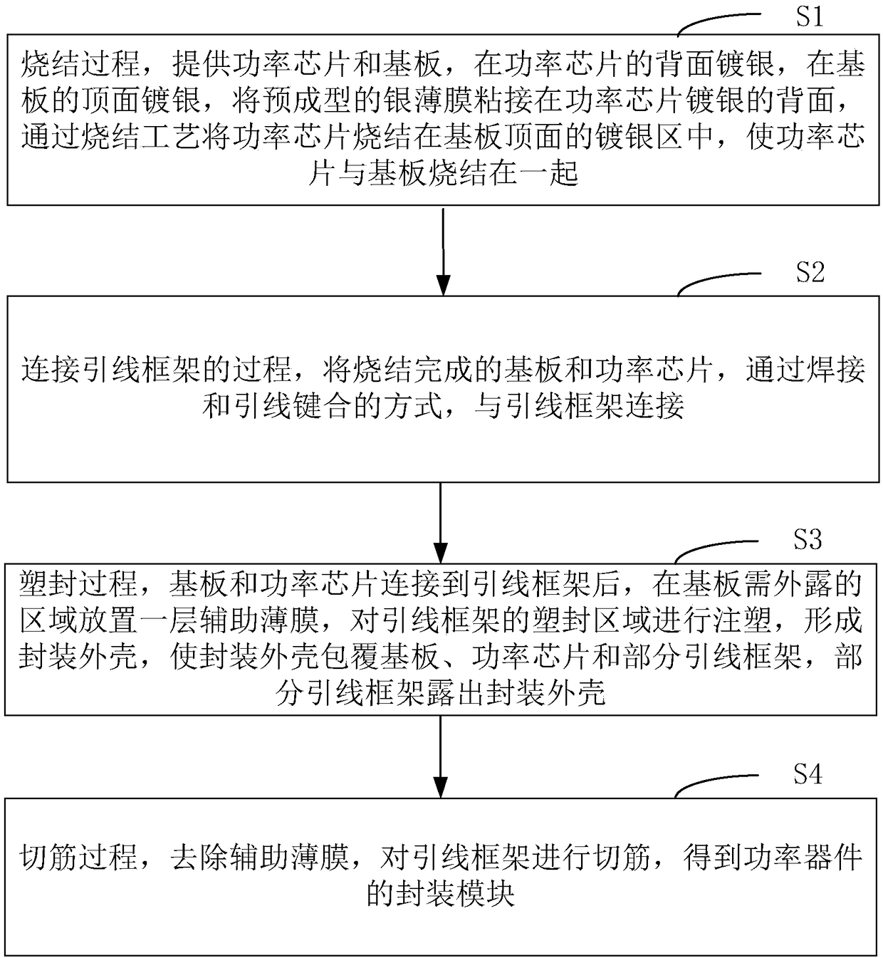
[0037] The invention provides a packaging method for a power device, combining figure 1 as shown, figure 1 It is a flow chart of the packaging method of the power device of the present invention, including the following steps:

[0038] Step S1: Sintering process, providing power chip and substrate, silver-plating on the back of the power chip, silver-plating on the top surface of the substrate, bonding the preformed silver film to the silver-plated back of the power chip, and sintering the power chip Sintered in the silver-plated area on the top surface of the substrate, the power chip is sintered with the substrate.

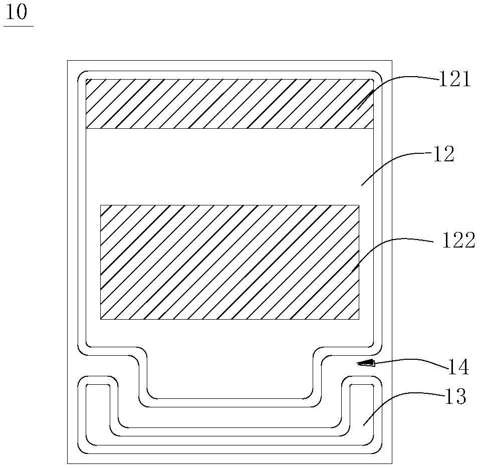
[0039] combine figure 2 as shown, figure 2A schematic diagram of the structure of the substrate. The substrate 10 may be made of silicon ni...


PUM


Abstract

The invention discloses a power device packaging method as well as a packaging module and a lead frame thereof. The packaging method comprises a sintering process, a lead frame connecting process, a plastic packaging process and a rib cutting process. The sintering process comprises the steps: adhering a silver film onto the silver-plated back of a power chip, and sintering the power chip in a silver plating area on the top of a substrate by using a sintering process. The substrate and the power chip subjected to sintering are connected with the lead frame in a manner of welding and lead bonding. During plastic packaging, an auxiliary film is arranged in a to-be-exposed area of the substrate, and the plastic packaging area of the lead frame is subjected to injection molding so as to form apackaging shell. The auxiliary film is removed, and the lead frame is subjected to rib cutting, thereby obtaining the power device packaging module. The power device packaging module is obtained by adopting the packaging method. According to the packaging method and the packaging module, the heat conduction performance between the power chip and the substrate is enhanced, and the product reliability is improved. A connecting line is formed between first source pins of the lead frame, and the connecting stability is improved.

Description

technical field [0001] The invention relates to the packaging field of semiconductor devices, in particular to a power device packaging method and its packaging module and lead frame. Background technique [0002] With the depletion of global oil resources and the increasing severity of the global greenhouse effect, countries around the world are vigorously developing a low-carbon economy. With the development of this trend, it has become inevitable for electric vehicles to replace fuel vehicles. At the same time, the requirements for packaging components used in automotive frequency conversion modules have also increased. However, the traditional plastic packaging process can no longer meet the power conversion requirements of high thermal conductivity, high input impedance, and low capacitance required in the field of electric vehicles. [0003] For example, in the traditional packaging process, the chip is usually fixed on the packaging platform through an adhesive materi...

Claims


Application Information

Patent Timeline
Patent Type & Authority Applications(China)
IPC IPC(8): H01L23/31H01L23/495H01L21/56
CPCH01L23/49575H01L21/561H01L23/3121H01L23/49537
Inventor 周福鸣刘军朱贤龙周泽雄
Owner SHENZHEN STS MICROELECTRONICS
Learn More