Back contact crystalline silicon heterojunction solar cell and preparation method thereof
A technology for solar cells and crystalline silicon, applied in the field of solar cells, can solve problems such as poor stability, and achieve the effect of simple process and suitable for large-scale production
- Summary
- Abstract
- Description
- Claims
- Application Information
AI Technical Summary
Problems solved by technology
Method used
Image
Examples
Embodiment 1
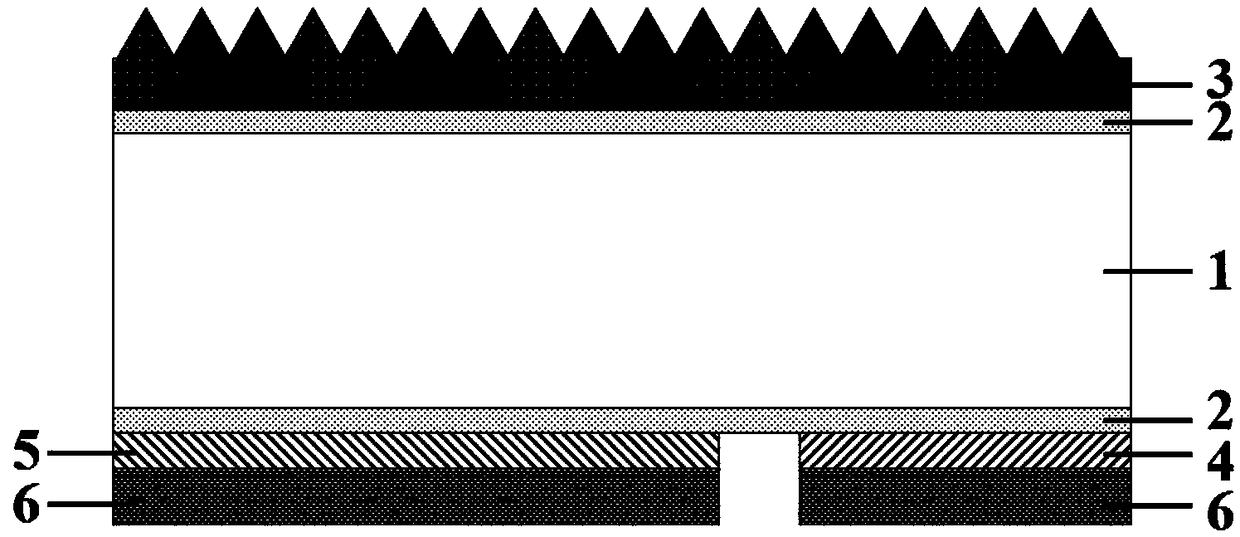
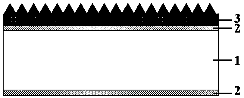
[0038] A back-contact crystalline silicon heterojunction solar cell, the solar cell comprising: a silicon substrate 1, a passivation layer 2, an antireflection film 3, a metal oxide reflector 4, a metal electrode 6, LiF x Film 5, the passivation layer 2 includes the first passivation layer and the second passivation layer, the material of the passivation layer 2 is SiO 2 .
[0039] The first passivation layer is deposited on the upper surface of the silicon substrate 1 .
[0040] The antireflection film is deposited 3 on the upper surface of the first passivation layer.
[0041] The second passivation layer is deposited on the lower surface of the silicon substrate 1, and the silicon substrate 1 is a single crystal silicon wafer.
[0042] The metal oxide reflector 4 is deposited on one end of the lower surface of the second passivation layer, and the LiF x A thin film 5 is deposited on the other end of the lower surface of the second passivation layer.
[0043] The metal e...
Embodiment 2
[0058] A back-contact crystalline silicon heterojunction solar cell, the solar cell comprising: a silicon substrate 1, a passivation layer 2, an antireflection film 3, a metal oxide reflector 4, a metal electrode 6, LiF x Film 5, the passivation layer 2 includes the first passivation layer and the second passivation layer, the material of the passivation layer 2 is Al 2 o 3 .
[0059] The first passivation layer is deposited on the upper surface of the silicon substrate 1 .
[0060] The antireflection film is deposited 3 on the upper surface of the first passivation layer.
[0061] The second passivation layer is deposited on the lower surface of the silicon substrate 1, and the silicon substrate 1 is a single crystal silicon wafer.
[0062] The metal oxide reflector 4 is deposited on one end of the lower surface of the second passivation layer, and the LiF x A thin film 5 is deposited on the other end of the lower surface of the second passivation layer.
[0063] The met...
PUM
 Abstract
Description
Claims
Application Information
 - R&D
- Intellectual Property
- Life Sciences
- Materials
- Tech Scout
- Unparalleled Data Quality
- Higher Quality Content
- 60% Fewer Hallucinations
Browse by: Latest US Patents, China's latest patents, Technical Efficacy Thesaurus, Application Domain, Technology Topic, Popular Technical Reports.
© 2025 PatSnap. All rights reserved.Legal|Privacy policy|Modern Slavery Act Transparency Statement|Sitemap|About US| Contact US: help@patsnap.com


