Power amplifier with electrostatic discharge protection circuit

An electrostatic discharge protection and power amplifier technology, which is applied to amplifiers with semiconductor devices/discharge tubes, amplifier protection circuit layout, amplifiers, etc. Ensure phase consistency, achieve output power, and improve the effect of protection level

Inactive Publication Date: 2018-07-24
天津大学(青岛)海洋工程研究院有限公司
View PDF10 Cites 1 Cited by
  • Summary
  • Abstract
  • Description
  • Claims
  • Application Information

AI Technical Summary

Problems solved by technology

[0003] At present, for the design of the electrostatic discharge protection circuit of the RF power amplifier, the main challenge is the interaction between the electrostatic discharge protection circuit and the core circuit.
The core circuit is very sensitive to any undesired parasitic effects, and the parasitic resistance and capacitance brought by the electrostatic discharge protection circuit will have a great impact on the input and output impedance matching, efficiency and bandwidth of the core circuit
The traditional electrostatic discharge protection circuit is realized by using a single electrostatic discharge protection device. The disadvantage of this method is that the area of ​​the electrostatic discharge protection device is large, the parasitic effect is strong, and the operating frequency is limited, which cannot meet the electrostatic discharge of the radio frequency power amplifier. protection requirements
Once the protection circuit is unreasonably designed, it will easily lead to circuit impedance mismatch, signal reflection, signal integrity is disturbed, and the power transmission efficiency from the signal input port to the core circuit is reduced
For the electrostatic discharge protection circuit of the narrowband RF power amplifier, the existing technology is to reduce the parasitic capacitance effect generated by the protection circuit through a simple matching network, but as the operating frequency of the RF power amplifier is getting higher and higher, especially in the working When the frequency exceeds several GHz, because the matching circuit itself also has strong parasitic effects, the simple method of reducing parasitic capacitance can no longer meet the design requirements

Method used


Image

  • Power amplifier with electrostatic discharge protection circuit
  • Power amplifier with electrostatic discharge protection circuit
  • Power amplifier with electrostatic discharge protection circuit

Examples


Embodiment Construction

[0016] In order to illustrate the technical solution of the present invention more clearly, the present invention will be further described below in conjunction with the accompanying drawings. For those skilled in the art, other drawings can also be obtained based on these drawings without creative effort.

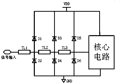
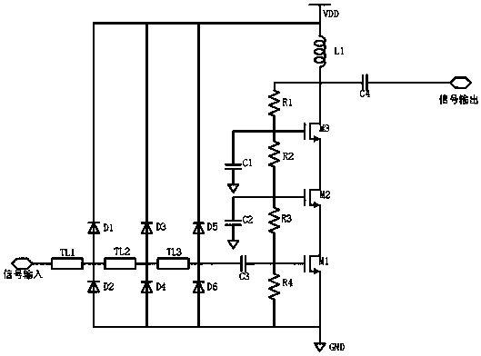
[0017] Such as figure 2 As shown, the core stack structure power amplifier of the present invention is composed of three NMOS transistors M1, M2, M3, the DC bias of each NMOS transistor is biased in class AB, and the resistors R1, R2, R3, and R4 are voltage dividing resistors , to provide bias voltage for the gates of the three NMOS transistors, and the bias point can be optimized by continuously adjusting the resistance ratio of the four resistors. The gates of the three NMOS transistors are respectively connected to three external capacitors C1, C2, and C3. The gate capacitances of the three NMOS transistors and the three external gate capacitors are used to adjust the...


PUM


Abstract

The invention relates to a power amplifier with an electrostatic discharge protection circuit. A core circuit uses a NMOS (N-channel metal oxide semiconductor) tube stacking structure; source electrodes and drain electrodes of three NMOS tubes are sequentially connected. Each NMOS tube is in bias arrangement in AB type; tandem resistors form a bias circuit. The electrostatic discharge protection circuit uses a distributed electrostatic discharge protection structure; the schematic diagram is shown as Figure 1; a diode in the protection circuit uses a PN junction diode; each electrostatic discharge protection unit uses the same diode; the diodes in parallel connection are connected through CPW (coplanar waveguide); the electrostatic discharge protection degrade of the core radio frequency power amplifier can be effectively improved; the parasitic effect of the protection circuit is weakened; the power amplifier is applicable to high work frequency.

Description

technical field [0001] The invention relates to an electrostatic discharge protection circuit, a radio frequency power amplifier and a power amplifier with an electrostatic discharge protection circuit in the field of integrated circuits. Background technique [0002] In the integrated circuit industry, electrostatic discharge (ESD) protection has become a serious problem for the reliability of integrated circuit products. From the manufacture and packaging of integrated circuits to assembly and transportation, there is always the danger of electrostatic discharge shocks. Many components are highly sensitive to electrostatic shock, and electrostatic discharge causes soft breakdown of the P / N junction of components, which greatly reduces the reliability of components. In addition, the lead wires in the chip are easily broken down by static electricity, which increases the scrap rate of the chip. During the transportation of integrated circuit chips, packaged chips without e...

Claims


Application Information

Patent Timeline
Patent Type & Authority Applications(China)
IPC IPC(8): H03F3/195H03F3/213H03F1/52
CPCH03F1/523H03F3/195H03F3/213
Inventor 马建国郭思成傅海鹏赵升
Owner 天津大学(青岛)海洋工程研究院有限公司
Why Eureka
Try Eureka