SCR electrostatic protection device and electrostatic protection circuit

An electrostatic protection and device technology, applied in the field of integrated circuit electrostatic protection, can solve the problems of inability to be directly applied, no parasitic transistors directly to the back substrate, no lateral devices, etc., and achieves low trigger voltage, low parasitic noise, and enhanced holding voltage. Effect

Inactive Publication Date: 2018-07-27
SEMICON MFG INT (SHANGHAI) CORP +1
View PDF5 Cites 14 Cited by
  • Summary
  • Abstract
  • Description
  • Claims
  • Application Information

AI Technical Summary

Problems solved by technology

However, the ESD device design used in bulk silicon CMOS cannot be directly applied to SOI CMOS technology, because the SCR (silicon controlled rectifier, silicon controlled rectifier) ​​directly formed due to the separation of the top layer silicon and the back substrate of the SOI structure No parasitic transistors through to the back substrate, nor lateral devices formed in the top silicon

Method used


Image

  • SCR electrostatic protection device and electrostatic protection circuit
  • SCR electrostatic protection device and electrostatic protection circuit
  • SCR electrostatic protection device and electrostatic protection circuit

Examples


Embodiment Construction

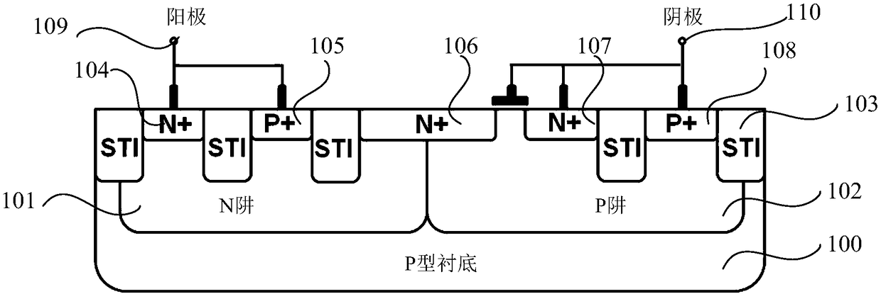
[0027] Please refer to figure 1 , figure 1 It is an existing LVTSCR device for ESD protection, formed in a bulk silicon substrate, specifically including: a P-type substrate 100, an N well 101, a P well 102, and a plurality of STI (Shallow Trench Isolation Structure) 103 , N+ doped regions 104, 106, 107, P+ doped regions 105, 108, wherein N well 101 and P well 102 are adjacent, N+ doped region 104 and P+ doped region 105 are formed in N well 101 and passed through an STI 103, the N+ doped region 106 is formed adjacent to the N well 101 and the P well 102, and is separated from the P+ doped region 105 by another STI 103, and the P+ doped region 108 and the N+ doped region 107 are formed in the P In the well 102 and separated by another STI 103, the N+ doped region 104 and the P+ doped region 105 are connected to the anode, the P well 102 between the N+ doped regions 106, 107 is covered with a gate electrode, the gate electrode, N+ The doped region 107 and the P+ doped region ...


PUM


Abstract

The invention provides an SCR electrostatic protection device and an electrostatic protection circuit. The SCR electrostatic protection device formed in a continuous active region of a top semiconductor layer on an insulating layer includes two N wells encircling a P doping region of an SCR and two P wells encircling an N doping region of the SCR to form a finger type diode structure, so that a parasitic PNP transistor and a parasitic NPN transistor of the SCR are formed; an additional N doping region adjacent to one N well and an additional P doping region adjacent to one P well are added between each two adjacent N well and P well and thus a parasitic gate controlled diode or PN junction diode is generated between the N well and the P well, so that the base electrode of the parasitic PNPtriode is connected to the base electrode of the parasitic NPN triode by the parasitic gate controlled diode or PN junction diode. According to the SCR electrostatic protection device and the electrostatic protection circuit, the low SCR trigger voltage and high maintaining voltage are provided and electrostatic protection is provided for the integrated circuit formed by processes like an SOI.

Description

technical field [0001] The invention relates to the technical field of electrostatic protection for integrated circuits, in particular to an SCR electrostatic protection device and an electrostatic protection circuit. Background technique [0002] Silicon-On-Insulator (SOI) introduces a buried oxide layer as an insulating layer between the top layer of silicon and the back substrate, and the buried oxide layer extends below the active region of the semiconductor element. SOI technology has brought many improvements in structure and physical characteristics, such as SOI structure has almost perfect sub-threshold swing (sub-threshold swing), no latch-up (latch-up free), low off-state leakage current (low off-state leakage), low operating voltage and high current drive capability, etc. However, the SOI structure also brings more serious electrostatic discharge (ESD) problems, especially for the three-dimensional FinFET SOI process, where the fin pitch and gate spacing have mad...

Claims


Application Information

Patent Timeline
Patent Type & Authority Applications(China)
IPC IPC(8): H01L27/02
CPCH01L27/0262
Inventor 陈光李宏伟
Owner SEMICON MFG INT (SHANGHAI) CORP
Why Eureka
Try Eureka