Method for improving bias voltage stability of TFT (Thin Film Transistor) with oxide insulating layer prepared by solution method

A technology of oxide insulating layer and insulating layer, which is applied in the manufacture of transistors, electrical components, semiconductors/solid-state devices, etc., can solve the problems of the decline of electrical properties of thin films, the crystallization state of insulating layer films, etc., and achieve the reduction of internal defects and surface roughness degree, good bias stability effect

Inactive Publication Date: 2018-07-31
SOUTH CHINA UNIV OF TECH
View PDF5 Cites 6 Cited by
  • Summary
  • Abstract
  • Description
  • Claims
  • Application Information

AI Technical Summary

Problems solved by technology

However, this method tends to cause the insulating layer film to appear crystalline, thereby degrading the electrical properties of the film.

Method used


Image

  • Method for improving bias voltage stability of TFT (Thin Film Transistor) with oxide insulating layer prepared by solution method
  • Method for improving bias voltage stability of TFT (Thin Film Transistor) with oxide insulating layer prepared by solution method
  • Method for improving bias voltage stability of TFT (Thin Film Transistor) with oxide insulating layer prepared by solution method

Examples


Embodiment 1

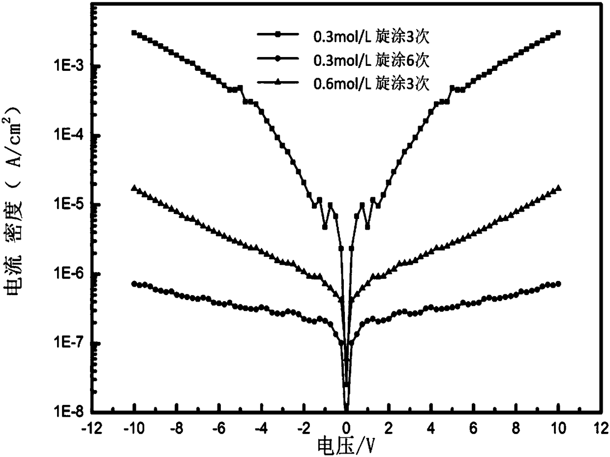
[0043] (1) Precursor preparation: 0.97g ZrOCl 2 ·8H 2 O (zirconium oxychloride octahydrate) was dissolved in 10ml ethylene glycol monomethyl ether (2-MOE), stirred and aged for 24h to obtain a 0.3mol / L precursor solution;

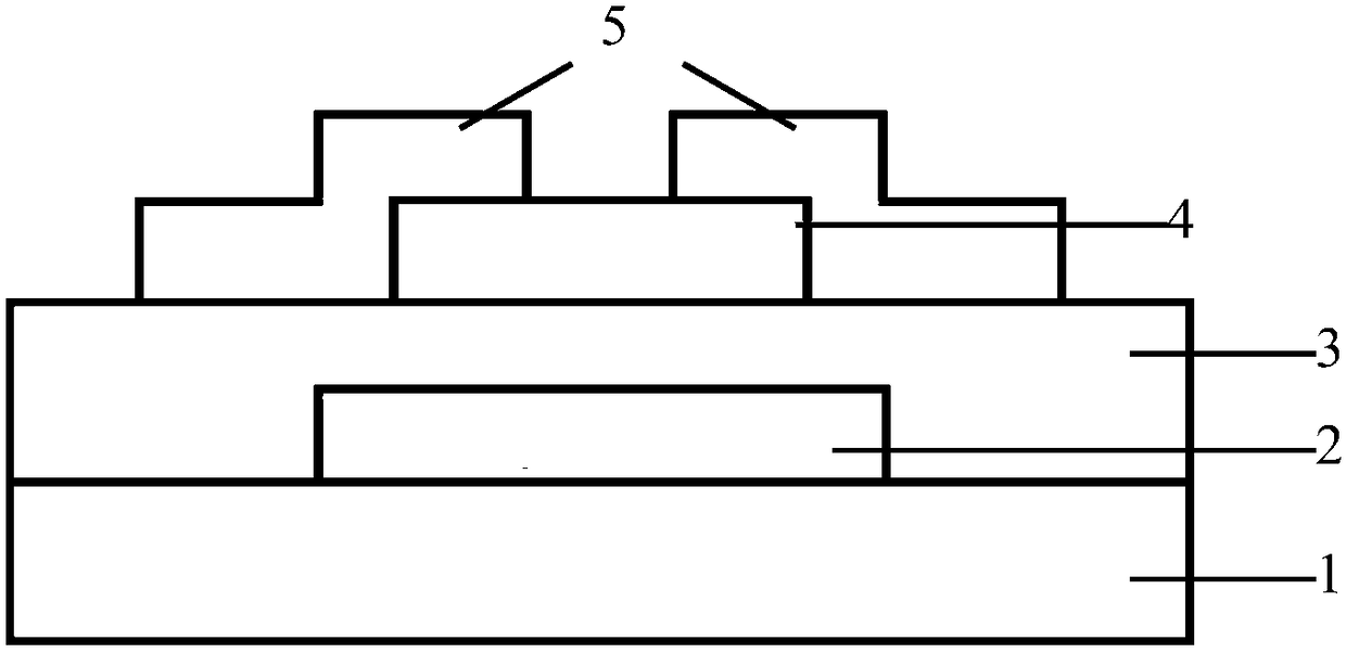
[0044] (2) Substrate preparation: deposit a layer of patterned ITO bottom gate (thickness is 150nm) on the surface of the glass substrate, wash and dry to obtain the ITO glass substrate;

[0045](3) On the ITO glass substrate (i.e. on the bottom grid), the precursor solution of step (1) is spin-coated multiple times (the spin-coating speed is 5000rpm, the number of times of spin-coating is 6 times, and the time of each spin-coating 40s (that is, the time for uniform glue)), annealing treatment (annealing at 300°C for 5min) after each spin coating, to obtain a metal oxide insulating layer film; then annealing the metal oxide insulating layer film at 350°C for 1h, to obtain Insulating layer; the metal oxide insulating layer film is a zirconia insulating lay...

Embodiment 2

[0048] Compared with Example 1, the concentration of the precursor solution is 0.26mol / L, the number of homogenization times is 7, the thickness of the insulating layer is 130nm, and other steps and conditions are completely the same.

Embodiment 3

[0050] Compared with Example 1, the concentration of the precursor solution is 0.2mol / L, the number of homogenization times is 9, and the thickness of the obtained zirconia insulating layer is 135nm. Other steps and conditions are completely the same.


PUM

PropertyMeasurementUnit
thicknessaaaaaaaaaa
thicknessaaaaaaaaaa
thicknessaaaaaaaaaa

Abstract

The invention belongs to the thin film transistor technical field and discloses a method for improving the bias voltage stability of a TFT (Thin Film Transistor) with an oxide insulating layer prepared by a solution method. According to the method of the invention, the insulating layer of the thin film transistor is prepared by means of spin-coating; a low-concentration metal oxide insulating layer precursor solution is subjected to spin-coating a plurality of times; annealing treatment is performed after spin coating is completed every time, so that a metal oxide insulating layer thin film isobtained; and the thin film is adopted as the insulating layer of the thin film transistor; and the concentration of the metal oxide insulating layer precursor solution ranges from 0 to 0.3 mol / L andis not 0. With the method of the present invention adopted, defects inside the insulating layer in the thin film transistor can be reduced, and the voltage bias stability of the thin film transistorcan be improved.

Description

technical field [0001] The invention belongs to the technical field of thin film transistors, and in particular relates to a method for improving the bias stability of a solution-processed oxide insulating layer TFT. Background technique [0002] A thin film transistor (Thin Film Transistor, TFT for short) is a semiconductor device with a wide range of uses, and its most important use is to drive liquid crystal alignment changes and drive OLED pixels to emit light in displays. When the oxide thin film transistor device is working on the display screen, the selection tube and the drive tube will be subjected to a long-term electrical bias, so whether the TFT device can maintain stable TFT device performance during the bias process will determine the effect of the backplane drive and service life. The metal oxide insulating film prepared by the solution method often contains many defects, which affects the bias stability of the TFT device. In order to solve this problem, the...

Claims


Application Information

Patent Timeline
Patent Type & Authority Applications(China)
IPC IPC(8): H01L29/786H01L21/445
CPCH01L21/445H01L29/66969H01L29/7869
Inventor 宁洪龙周尚雄姚日晖蔡炜陶瑞强陈建秋朱镇南魏靖林刘贤哲彭俊彪
Owner SOUTH CHINA UNIV OF TECH
Why Eureka
Try Eureka