Manufacturing process of silicon solar cell

A solar cell and manufacturing process technology, applied in sustainable manufacturing/processing, final product manufacturing, circuits, etc., can solve the problems that MWT solar cells cannot further improve conversion efficiency, and cannot cover uniformly perforated side walls, so as to improve photoelectric conversion Efficiency, improvement of battery conversion efficiency, and cost reduction

Inactive Publication Date: 2018-07-31
JIANGSU MICROVIA NANO EQUIP TECH CO LTD
View PDF8 Cites 4 Cited by
  • Summary
  • Abstract
  • Description
  • Claims
  • Application Information

AI Technical Summary

Problems solved by technology

[0007] In order to solve the Al 2 o 3 technology, the perforated sidewall cannot be uniformly covered, resulting in the inability of the MWT solar cell to fur

Method used


Image

  • Manufacturing process of silicon solar cell
  • Manufacturing process of silicon solar cell
  • Manufacturing process of silicon solar cell

Examples


Embodiment 1

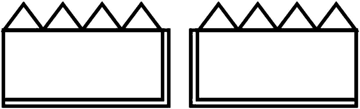
[0052] Such as figure 1 As shown, the ALD film is prepared on the perforated inner wall and the back of the battery, and the back of the battery and the perforated inner wall (reaction in figure 1 Among them, the inner wall of the perforation (the gap in the middle of the battery) has a uniform coating, which can effectively passivate the back of the p-type crystalline silicon battery, and at the same time protect the hole wall and insulate the front and back electrodes.

[0053] process such as Figure 4 Shown are: Laser Drilling, Texturing, Diffusion, Reverse Etching, ALD or PEALD passivation, Front AR, Printing, Sintering.

[0054] (1) Laser drilling: use a P-type single crystal silicon wafer with a resistivity of 1 to 3Ω.cm as the substrate, and use a laser to drill several columns from the back of the silicon wafer with a diameter of 1.2 to 2.2mm. The spacing is 8-20mm;

[0055] (2) Texturing: Texturing the silicon wafer, and making a P-N junction with a square resista...

Embodiment 2

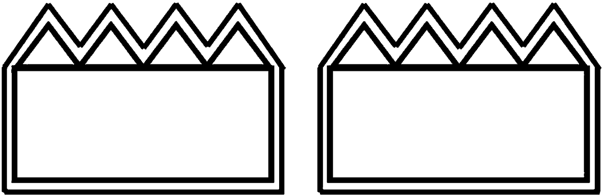
[0063] Such as figure 2 As shown, the ALD film was prepared by perforating the inner wall and the front and back of the battery (reaction in figure 2 Among them, the inner wall of the perforation is the gap in the middle of the battery), which can effectively passivate the back of the p-type crystalline silicon battery, and at the same time protect the wall and front of the hole and insulate the front and back electrodes.

[0064] process such as Figure 5 Shown: laser drilling, texturing, diffusion, back etching, front anti-reflection layer, ALD or PEALD passivation film, printing, sintering.

[0065] (1) Laser drilling: use a P-type single crystal silicon wafer with a resistivity of 1 to 3Ω.cm as the substrate, and use a laser to drill several columns from the back of the silicon wafer with a diameter of 1.2 to 2.2mm. The spacing is 8-20mm;

[0066] (2) Texturing: Texturing the silicon wafer, and making a P-N junction with a square resistance value of 85-95Ω / port on the...

Embodiment 3

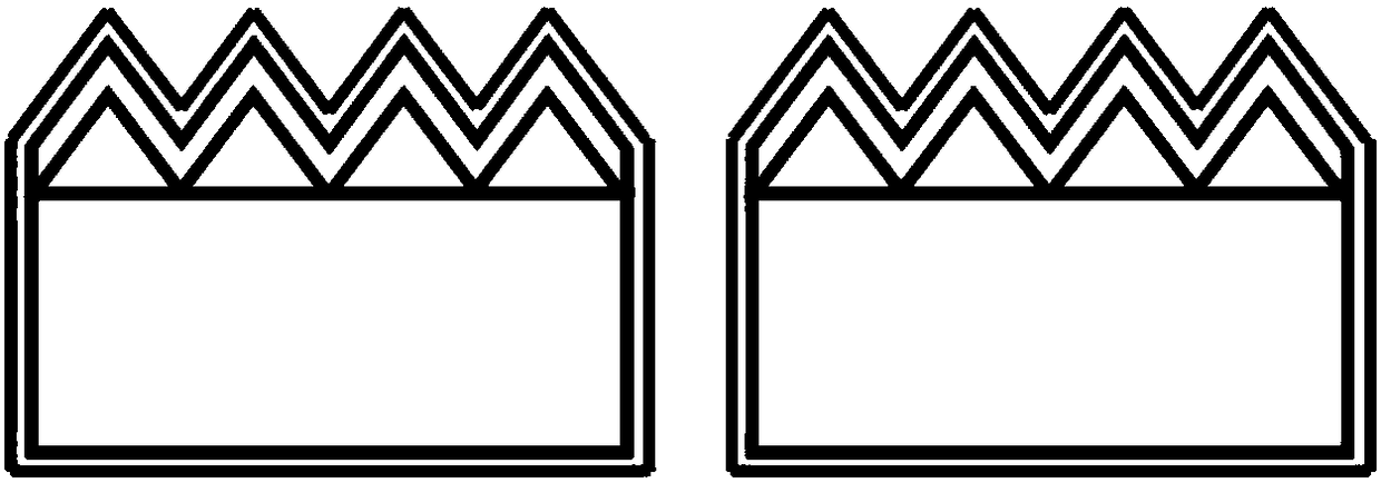
[0074] Such as image 3 As shown, ALD film is prepared on the front and back of the perforated inner wall and coated with oxide film or anti-reflection film battery (reaction in image 3 Among them, the inner wall of the perforated hole is the gap in the middle of the battery), which can effectively passivate the back of the p-type crystalline silicon battery, and at the same time protect the hole wall and front side and insulate the front and back electrodes.

[0075] process such as Figure 6 Shown: laser drilling, texturing, diffusion, back etching, oxide layer, front anti-reflection layer, ALD or PEALD passivation film, printing, sintering.

[0076] (1) Laser drilling: A P-type single crystal silicon wafer with a resistivity of 1-3Ω.cm is selected as the substrate, and a laser is used to open several rows of holes from the back of the silicon wafer. The diameter of the holes is 1.2-2.2mm. The spacing is 8-20mm;

[0077] (2) Texturing: Texturing the silicon wafer, and ma...


PUM

PropertyMeasurementUnit
Thicknessaaaaaaaaaa
Thicknessaaaaaaaaaa
Resistivityaaaaaaaaaa

Abstract

The present invention discloses a manufacturing process of a silicon solar cell. The manufacturing process of the silicon solar cell comprises the following processes of: laser drilling, texture surface making, diffusion, back etching, atomic layer deposition or plasma atomic layer deposition passivation coating, front antireflection layer coating and printing sintering. The laser drilling can beperformed prior to or after any one of the processes of texture surface making, diffusion and back etching. The process sequence of the atomic layer deposition or the plasma atomic layer deposition passivation coating and the front antireflection layer coating can be regulated according to the process requirement. The atomic layer deposition or the plasma atomic layer deposition process is employed to perform coating at one side of a battery piece or at the inner wall of a through hole, or the atomic layer deposition or the plasma atomic layer deposition process is employed to perform coatingat the two sides of the battery piece and at the inner wall of the through hole.

Description

technical field [0001] The invention relates to the manufacture of crystalline silicon solar cells, in particular to the passivation process for crystalline silicon solar cells by atomic layer deposition (ALD) technology. Background technique [0002] The metallization wrap-through (MWT) silicon solar cell was proposed by Solland Solar, a Dutch solar cell manufacturer. Due to its theoretically lower production cost and compatibility with various solar cell process advantages, MWT solar cell technology is praised by industry experts as the best platform technology to change the future of photovoltaic manufacturing, which is both efficient and cost-effective. With the continuous development of modern science and technology, it will gradually replace conventional technology in the near future and become the development direction of future industrialization. [0003] MWT solar cell technology adopts the technology of laser drilling and rear wiring to eliminate the main grid lin...

Claims


Application Information

Patent Timeline
IPC IPC(8): H01L31/18H01L31/0216H01L31/028
CPCH01L31/02168H01L31/028H01L31/1804Y02E10/547Y02P70/50
Inventor 黎微明糜珂
Owner JIANGSU MICROVIA NANO EQUIP TECH CO LTD
Why Eureka
Try Eureka