Photovoltaic solder strip, preparation method therefor, and photovoltaic assembly

A photovoltaic ribbon and tin soldering technology, which is applied in photovoltaic power generation, electrical components, semiconductor devices, etc., can solve the problems of no obvious improvement in welding effect, increased cost, and large changes in solder composition, so as to ensure the repair rate of components, Good welding tension and improved photoelectric conversion efficiency

Active Publication Date: 2018-08-03
JINKO SOLAR CO LTD +1
View PDF6 Cites 6 Cited by
  • Summary
  • Abstract
  • Description
  • Claims
  • Application Information

AI Technical Summary

Problems solved by technology

However, on the basis of conventional photovoltaic ribbons, the solder composition of these photovoltaic ribbons has ...

Method used


Image

  • Photovoltaic solder strip, preparation method therefor, and photovoltaic assembly
  • Photovoltaic solder strip, preparation method therefor, and photovoltaic assembly
  • Photovoltaic solder strip, preparation method therefor, and photovoltaic assembly

Examples


preparation example Construction

[0046] The invention provides a method for preparing a photovoltaic ribbon, which is characterized in that it comprises:

[0047] A) heating, melting and mixing tin, lead, gallium and bismuth raw materials to obtain a molten liquid;

[0048] B) Contacting the surface of the conductive base tape with the molten liquid to obtain a photovoltaic soldering tape.

[0049] The preparation method of the photovoltaic ribbon provided by the present invention first heats, melts and mixes tin, lead, gallium and bismuth raw materials to obtain a melt.

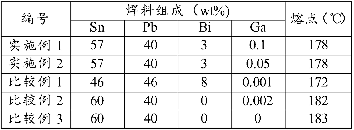
[0050] According to the present invention, the mass ratio of the tin, lead, gallium and bismuth is preferably (55-65): (35-45): (0.0005-0.5): (1-5); more preferably (56-63) : (36-43): (0.01-0.3): (1-4); most preferably (56-58): (38-40): (0.01-0.05): (2-4).

[0051] The present invention does not limit its source, and it can be commercially available.

[0052] The present invention does not limit the specific manner of the heating and mel...

Embodiment 1~2

[0061] As shown in Table 1, mix the raw materials evenly to form a solder layer and melt it, then dip a copper strip with a thickness of 0.3 mm and a width of 1.5 mm in the molten liquid, and pass through the air knife device to obtain photovoltaic ribbons in sequence. Wherein, the thickness of the solder layer on the upper and lower surfaces of the copper base strip is 23±4um.


PUM

PropertyMeasurementUnit
Thicknessaaaaaaaaaa
Widthaaaaaaaaaa
Thicknessaaaaaaaaaa

Abstract

The invention provides a photovoltaic solder strip, and the solder strip comprises a conductive base strip and a tin soldering layer wrapping the conductive base strip. The tin soldering layer contains 55-65wt% of Sn, 35-45wt% of Pb, 1-5wt% of Bi, and 0.0005-0.5wt% of Ga. According to the invention, the soldering flux is formed by the four materials of Sn-Pb-Bi-Ga at a specific proportion. In particular, the melting point of the soldering flux is 145-170 DEG C after the Bi and Ga elements are added. The method can maintain the better soldering tension while achieving the low-temperature welding, and guarantees the ideal repair rate of the assembly. In addition, the photoelectric conversion efficiency of the photovoltaic assembly of the photovoltaic solder strip provided by the invention iseffectively improved.

Description

technical field [0001] The invention relates to the field of manufacturing crystalline silicon solar modules, in particular to a method for preparing a photovoltaic welding ribbon and a photovoltaic module. Background technique [0002] The crystalline silicon solar cell itself is relatively brittle, and the solar module includes multiple cells, which are connected by copper-based photovoltaic ribbons. The common solder layer composition in photovoltaic ribbons is 60% Sn, 40% Pb. In the phase diagram, the eutectic point temperature of the Sn-Pb alloy is about 183°C, that is, the melting point of the solder layer in the photovoltaic ribbon is 183°C, but in the actual welding process, the welding temperature is higher than the melting point of the solder by more than 20°C. During the welding process, the battery sheet is warped and deformed greatly, and the risk of hidden cracks after welding is high, and the fragmentation rate is high. Especially for PERC single crystal, its...

Claims


Application Information

Patent Timeline
IPC IPC(8): H01L31/05H01L31/18
CPCH01L31/0512H01L31/1804Y02E10/547Y02P70/50
Inventor 赵钟轩占卫君杨川李楠黄骏孙岳懋
Owner JINKO SOLAR CO LTD
Why Eureka
Try Eureka