High-performance perovskite/organic semiconductor heterojunction type photoelectric detector

A technology of organic semiconductors and photodetectors, applied in semiconductor devices, semiconductor/solid-state device manufacturing, photovoltaic power generation, etc., can solve the problems of small photocurrent response, high working voltage, complex structure, etc., achieve good application potential, and suppress impact , the effect of photoelectric response enhancement

Inactive Publication Date: 2018-08-03
FUDAN UNIV
View PDF3 Cites 7 Cited by
  • Summary
  • Abstract
  • Description
  • Claims
  • Application Information

AI Technical Summary

Problems solved by technology

Although the conventional p-i-n structure perovskite photodetector has a simple structure and low working voltage, its photocurrent response is small, while the perovskite based on the field effect tube type has a large photoelectric response, but the working voltage is high. complex structure
Therefore, the performance of photodetectors with these structures has its own shortcomings, which limits the practical application of perovskite photodetectors to a certain extent.

Method used


Image

  • High-performance perovskite/organic semiconductor heterojunction type photoelectric detector

Examples


Embodiment 1

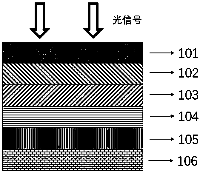
[0025] Schematic diagram of the structure of a high-performance perovskite / organic semiconductor heterojunction photodetector. figure 1 Shown: 101 is the transparent substrate BK7 glass, 102 is the transparent bottom electrode ITO, the thickness is 110 nanometers, 103 is the hole transport layer CuPC, the thickness is 50nm, 104 is the perovskite light-absorbing layer, the thickness is 300 nanometers, 105 empty The hole transport layer CuPC has a thickness of 50 nanometers, and 106 is a metal top electrode with a thickness of 80 nanometers.

[0026] The preparation method of perovskite / organic semiconductor heterojunction photodetector in Example 1 is as follows:

[0027] The ITO bottom electrode layer is formed by sputtering coating on BK7 glass, and the square resistance is less than 10Ω / □. Transfer the substrate into a vacuum chamber to grow 50 nm CuPc. Then put it into the glove box, dissolve MAI / PbI2 with a molar ratio of 1:1 in DMF to form a 40wt% CH3NH3PbI3 precursor s...

Embodiment 2

[0028] Embodiment 2, the preparation method of perovskite / organic semiconductor heterojunction photodetector is as follows:

[0029] The ITO bottom electrode layer is formed by sputtering coating on BK7 glass, and the square resistance is less than 10Ω / □. Into the glove box, spin-coat 4wt% Spiro-OMeTAD solution on the substrate at a speed of 4000RPM, anneal at 100 degrees Celsius for five minutes, and the film thickness is about 80nm. Dissolve MAI / PbI2 with a molar ratio of 1:1 in DMF to form a 40wt% CH3NH3PbI3 precursor solution, spin-coat at 3000RPM for 60 seconds, and anneal at 100 degrees for 5min to form a perovskite film with a thickness of about 280 nm . Then continue to use 4wt% Spiro-OMeTAD solution to spin-coat on the perovskite film at a speed of 4000RPM, with a thickness of about 80nm. The substrate is introduced into the vacuum chamber, and 80nm gold electrodes are grown to complete the preparation of the device.


PUM


Abstract

The invention relates to a high-performance perovskite/organic semiconductor heterojunction type photoelectric detector, and belongs to the technical field of semiconductor photoelectric devices. Thephotoelectric detector prepared via a lamination technology structurally comprises a transparent bottom electrode layer, an organic semiconductor and perovskite function layer and a top electrode layer successively from bottom to top; the organic semiconductor and perovskite function layer includes a cavity type organic semiconductor, perovskite and another cavity type organic semiconductor, or anelectronic type organic semiconductor, perovskite and another electronic organic semiconductor successively from bottom to to; the perovskite and organic semiconductor layer form two heterojunctions;and the top electrode is made of gold or silver. The photoelectric detector is wide in response spectrum and simple in structure, can make response to visible spectrums in full waveband, and has a voltage saturation characteristic, the working voltage is 0.7V, and influence of voltage noise on performance of the detector can be inhibited effectively.

Description

technical field [0001] The invention belongs to the technical field of semiconductor optoelectronic devices, in particular to the field of perovskite / organic semiconductor photodetectors. Background technique [0002] Organic-inorganic hybrid perovskite materials combine the excellent properties of traditional semiconductors and new organic semiconductors. Compared with new organic semiconductor materials, organic-inorganic hybrid perovskite materials have higher mobility; compared with traditional inorganic semiconductors, organic-inorganic perovskite materials have simple preparation, low cost, and adjustable energy bands. , flexibility and many other advantages. Therefore, it has high application potential in the field of optoelectronics, especially in photoelectric sensors. Although the conventional p-i-n structure perovskite photodetector has a simple structure and low working voltage, its photocurrent response is small, while the perovskite based on the field effect ...

Claims


Application Information

Patent Timeline
Patent Type & Authority Applications(China)
IPC IPC(8): H01L51/42H01L51/48
CPCH10K71/12H10K30/10Y02E10/549
Inventor 詹义强袁斯建
Owner FUDAN UNIV
Why Eureka
Try Eureka