Multi-chip wafer level fan-out type three-dimensional package structure and packaging process thereof

A three-dimensional, packaging structure technology, applied in the direction of electric solid-state devices, semiconductor devices, semiconductor/solid-state device manufacturing, etc., can solve the problems of large packaging area, poor precision, and inability to achieve multi-function, etc., to reduce the packaging area and improve integration degree of effect

Pending Publication Date: 2018-08-10
王新
View PDF7 Cites 10 Cited by
  • Summary
  • Abstract
  • Description
  • Claims
  • Application Information

AI Technical Summary

Problems solved by technology

[0004] Purpose of the invention: The purpose of the present invention is to solve the existing packaging requirements of electronic devices that can integrate chips with different functions. However, the p

Method used


Image

  • Multi-chip wafer level fan-out type three-dimensional package structure and packaging process thereof
  • Multi-chip wafer level fan-out type three-dimensional package structure and packaging process thereof
  • Multi-chip wafer level fan-out type three-dimensional package structure and packaging process thereof

Examples


Embodiment 1

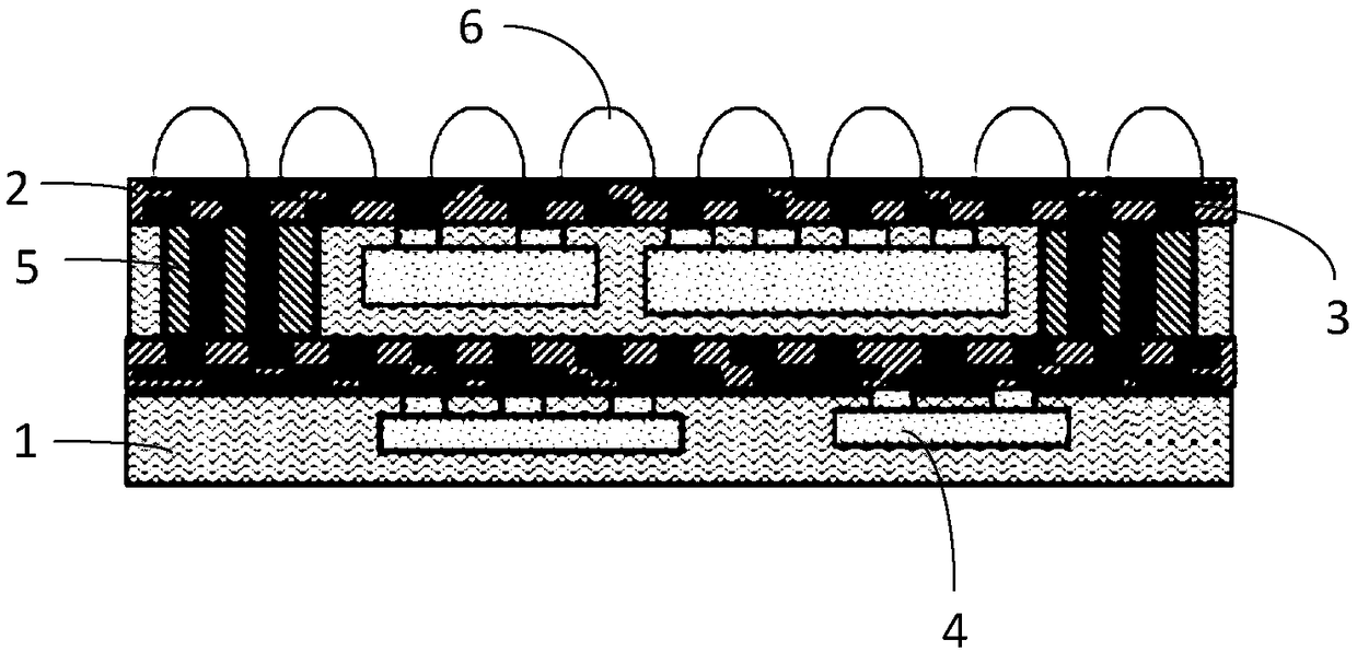
[0066] as attached figure 1 As shown, an integrated packaging structure includes two rewiring layers, the rewiring layer is a dielectric layer 2, and the plastic sealing layer 1, the dielectric layer 2, the plastic sealing layer 1 and the dielectric layer 2 are arranged in sequence from top to bottom, On both sides of the dielectric layer 2, there is a metal connection structure 3 that connects the two sides to cooperate with each other and form an interconnected structure. One end of the metal connection structure 3 is parallel to the plane of the dielectric layer 2, and one end extends out of the dielectric layer 2. The metal contact (not shown) side of the dielectric layer 2 is provided with a plastic sealing layer 1, and a chip 4 (including a bare chip, a packaged chip, etc.) or a passive passive component (not shown) is plastic sealed in the plastic sealing layer 1 , the plastic sealing layer 1 between the two dielectric layers 2 is also provided with a micro-silicon bloc...

Embodiment 2

[0076] An integrated packaging structure, including three layers of rewiring layers, the rewiring layer is a dielectric layer 2, and the plastic packaging layer 1, the dielectric layer 2, the plastic packaging layer 1, the dielectric layer 2, and the plastic packaging layer 1 are arranged in sequence from top to bottom and the dielectric layer 2, on both sides of the dielectric layer 2, there is a metal connection structure 3 that connects the two sides to cooperate with each other and form an interconnected structure. One end of the metal connection structure 3 is parallel to the plane of the dielectric layer 2, and one end extends out The dielectric layer 2 is provided with a plastic sealing layer 1 on one side of the metal contact (not shown) extending out of the dielectric layer 2, and a chip 4 (including a bare chip, a packaged chip, etc.) or a passive passive Components (not shown), the plastic sealing layer 1 between two adjacent dielectric layers 2 is also provided with...

Embodiment 3

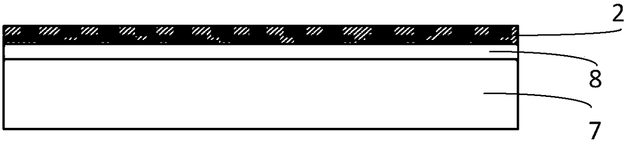
[0086] A packaging process for a multi-chip wafer-level fan-out three-dimensional packaging structure as claimed in claim 1, comprising the following steps:

[0087] 1) Adhering a temporary bonding adhesive layer 8 on the surface of the temporary carrier 7;

[0088] The temporary carrier is a light-transmitting carrier (such as quartz, glass, etc.) or an opaque carrier (such as metal, silicon wafer, ceramics, etc.), and the temporary bonding adhesive layer is thermal peeling glue, UV glue or laser Debonding glue.

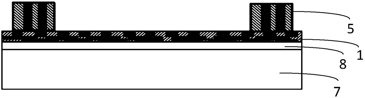
[0089] 2) The surface of the temporary bonding adhesive layer 8 obtained in step 1) is used to make the first layer of rewiring layer with a thin film process. The metal connection structure 3 that cooperates with each other and forms an interconnected structure;

[0090] It is used to interconnect chips and passive components to be packaged in subsequent steps and lead out the formed pins.

[0091] The production of the rewiring layer specifically includes the f...


PUM


Abstract

The invention relates to a multi-chip wafer level fan-out type three-dimensional package structure, comprising at least two rewiring layers, wherein the rewiring layers are dielectric layers, metal connecting structures connected with two sides to match each other and form interconnecting structures are provided on two sides of the dielectric layers, the metal connecting structures expose the dielectric layers to form metal contacts, a plastic sealing layer is arranged on one side of the rewiring layers, chips or passive elements are packaged in the plastic sealing layer, and the adjacent rewiring layers are connected by micro silicon blocks. The invention also discloses a packaging process for the multi-chip wafer level fan-out type three-dimensional package structure. By adopting the design scheme, passive devices of different sizes can be simultaneously integrated and packaged with bare chips, so that the degree of integration is greatly improved, the packaging process is particularly suitable for application of wifi, PA, PMU and the like using a large number of passive devices, and at the same time, the three-dimensional stacking method greatly reduces the packaging area.

Description

technical field [0001] The invention relates to the technical field of semiconductor packaging, in particular to a multi-chip wafer-level fan-out three-dimensional packaging structure and a packaging process thereof. Background technique [0002] With the increasing multi-functionality and miniaturization of electronic devices, the types and quantities of chips that need to be integrated and packaged are also increasing. For example, applications such as wifi / PA / PMU need to integrate active chips (bare Chips, or packaged chips, etc.) are assembled with other devices such as passive passive components to realize a single package with certain functions, thus forming a system or subsystem. [0003] The currently widely used fan-out packaging is to rewire all the passive components and bare chips that have been plastic-packed together to achieve interconnection packaging between components. In the integrated packaging of complex and diverse chips and passive passive devices, th...

Claims


Application Information

Patent Timeline
IPC IPC(8): H01L21/683H01L23/31H01L23/498H01L25/16H01L21/48H01L21/56
CPCH01L23/49838H01L25/16H01L21/4853H01L21/56H01L21/6835H01L23/3185H01L2221/68345H01L2224/81005H01L2924/15313H01L2924/3511H01L2224/16225
Inventor 王新蒋振雷陈坚
Owner 王新
Why Eureka
Try Eureka