Method for forming self-aligned contact hole

A self-aligned contact hole and self-alignment technology, applied in the direction of electrical components, semiconductor/solid-state device manufacturing, circuits, etc., can solve the problems such as easy to shift to the top of the field oxygen 102, the process capacity cannot be reduced, and other problems

Active Publication Date: 2018-08-17
SHANGHAI HUAHONG GRACE SEMICON MFG CORP
View PDF4 Cites 2 Cited by
  • Summary
  • Abstract
  • Description
  • Claims
  • Application Information

AI Technical Summary

Problems solved by technology

[0006] As the size of the device continues to shrink, the size of the active region will also continue to shrink, but the size of the contact hole 104 on the top layer cannot be reduced in the same proportion due to process capability issues.
In this way, the size of the contact hole 104 will be relatively large, and a photolithographic offset will inevitably occur in the photolithography process corresponding to the contact hole 104. Since the contact hole 104 will be in contact with the surface of the active region under normal conditions, as As the size of the device decreases, the photolithography offset of the contact hole 104 is easily shifted to the top of the field oxygen 102; in this way, the field oxygen 102 at the bottom will also be etched during the subsequent etching of the interlayer film 103, and finally When the metal is filled, the metal in the contact hole 104 penetrates deep into the field oxygen 102, as shown by the mark 105. When the depth is deep, it will cause leakage and reliability problems of the device.

Method used


Image

  • Method for forming self-aligned contact hole
  • Method for forming self-aligned contact hole
  • Method for forming self-aligned contact hole

Examples


Embodiment Construction

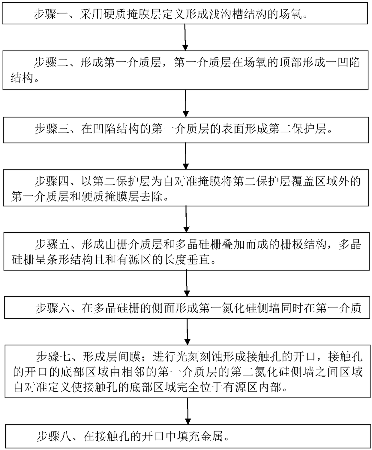
[0055] Such as figure 2 Shown is a flowchart of a method for forming a self-aligned contact hole 7 according to an embodiment of the present invention; Figure 3 to Figure 8B As shown, it is a schematic diagram of the device structure in each step of the method of the embodiment of the present invention. The method for forming the self-aligned contact hole 7 of the embodiment of the present invention includes the following steps:

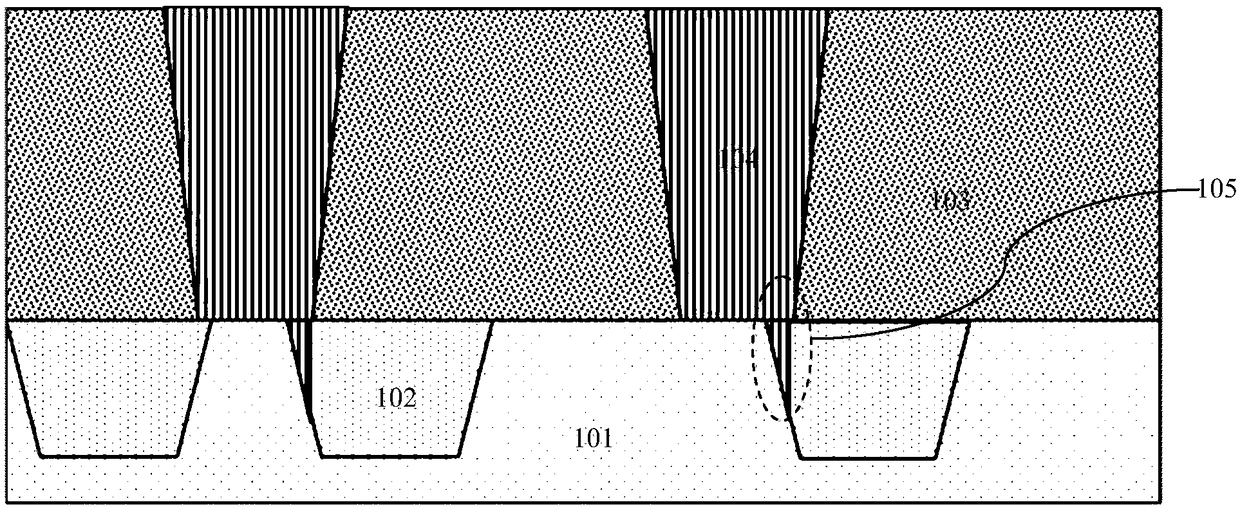
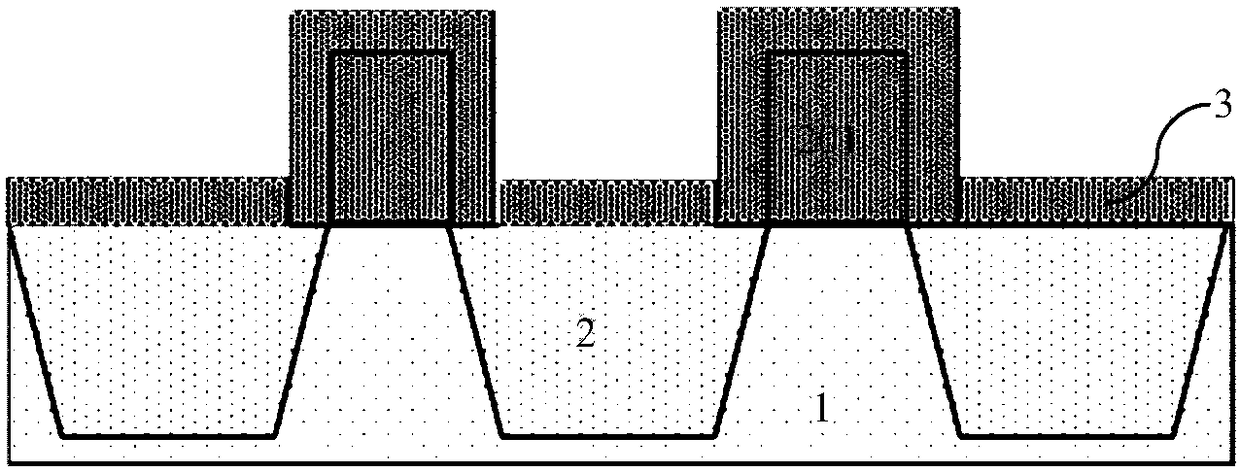
[0056] Step 1, such as image 3 As shown, a shallow trench is formed on the semiconductor substrate 1 and field oxygen 2 is filled in the shallow trench, and the active region is isolated by the field oxygen 2, that is, the active region is isolated by the field oxygen 2 The composition of the semiconductor substrate 1. Each of the active regions has a strip structure and is arranged in parallel; the etching area of ​​the shallow trench is defined by a hard mask layer 201 covering the surface of the active region.

[0057] In the embodiment of t...


PUM


Abstract

The invention discloses a method for forming a self-aligned contact hole. The method comprises the steps of defining field oxide of forming a shallow trench structure by adopting a hard mask layer; forming a first dielectric layer; forming a second protection layer on the surface of the first dielectric layer with a sag structure; removing the first dielectric layer and the hard mask layer outsidethe area covered with the second protection layer by adopting the second protection layer as a self-aligned mask; forming a gate structure; forming a first silicon nitride side wall on the side surface of a polysilicon gate, simultaneously forming a second silicon nitride side wall on the side surface of the first dielectric layer and covering an active area and the boundary of the field oxide with the second silicon nitride side wall; forming an interlayer film; carrying out photoetching to form an opening of the contact hole; and filling the opening of the contact hole with metal. Accordingto the method, the bottom area of the contact hole can be located in the active area in a self-aligned manner, so that the bottom of the contact hole is prevented from deviating to the field oxide, generated electric leakage of a device can be prevented and the reliability of the device can be improved.

Description

technical field [0001] The invention relates to a semiconductor integrated circuit manufacturing process method, in particular to a method for forming a self-aligned contact hole. Background technique [0002] In the integrated circuit manufacturing process, with the continuous reduction of device size, in order to reduce the size of the device, the size of the active region needs to be continuously reduced. Due to the problem of process capability, the size of the contact hole cannot be reduced accordingly, and there are often contact holes. The hole falls in the case of a smaller active area, and due to fluctuations between processes, the contact hole will fall in the shallow trench isolation area, that is, the shallow trench field oxygen. [0003] Since the contact hole needs to pass through the interlayer film composed of silicon dioxide, and the dielectric layer of the shallow trench field oxygen is also silicon dioxide, the shallow trench field oxygen will be generated...

Claims


Application Information

Patent Timeline
Patent Type & Authority Applications(China)
IPC IPC(8): H01L21/768
CPCH01L21/76897
Inventor 郭振强
Owner SHANGHAI HUAHONG GRACE SEMICON MFG CORP
Why Eureka
Try Eureka