Protection device for power component, and manufacturing method thereof

A technology for protecting devices and power components, which is applied in the manufacture of semiconductor/solid-state devices, electrical components, and electro-solid devices, etc. The effect of reducing production costs

Active Publication Date: 2018-08-17
NANJING HENGZHONG MECHANISM TECH
View PDF6 Cites 1 Cited by
  • Summary
  • Abstract
  • Description
  • Claims
  • Application Information

AI Technical Summary

Problems solved by technology

[0005] In view of this, the object of the present invention is to provide a protection device for power components and its manufacturing method, so as to alleviate the technical problems of low anti-surge capability and large device area in the prior art

Method used


Image

  • Protection device for power component, and manufacturing method thereof
  • Protection device for power component, and manufacturing method thereof
  • Protection device for power component, and manufacturing method thereof

Examples


Embodiment 1

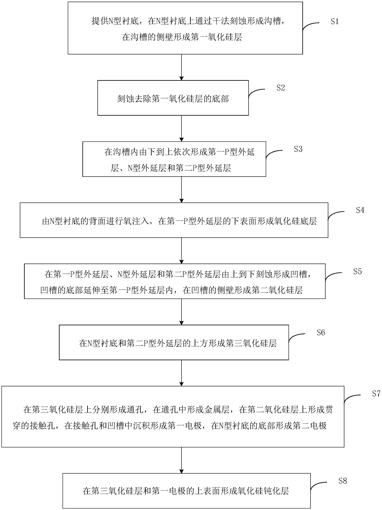
[0038] see figure 1 , a flowchart of a method for manufacturing a protection device for a power element provided by an embodiment of the present invention. A method for manufacturing a protection device for a power element provided by an embodiment of the present invention includes the following steps:

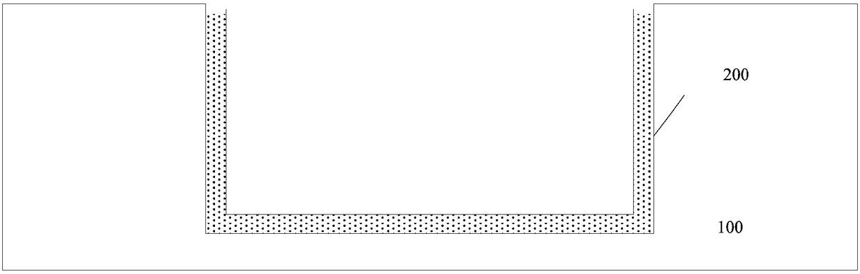
[0039]Step 1: An N-type substrate 100 is provided, a trench is formed on the N-type substrate by dry etching, and a first silicon oxide layer 200 is formed on the sidewall of the trench. see figure 2 , a product schematic diagram of Step 1 in the method for manufacturing a protection device for a power element provided in an embodiment of the present invention.

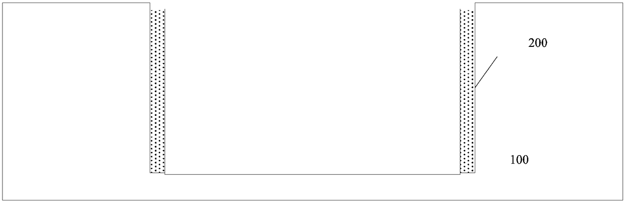
[0040] Step 2: Etching and removing the bottom of the first silicon oxide layer. see image 3 , a product schematic diagram of Step 2 in the method for manufacturing a protection device for a power element provided in an embodiment of the present invention.

[0041] Step 3: Form a first P-type epitaxial layer 51...

Embodiment 2

[0052] An embodiment of the present invention provides a protection device for a power element. The protection device for a power element is prepared according to the above method for manufacturing a protection device for a power element, and includes: an N-type substrate 100, a first silicon oxide layer 200, and a silicon oxide bottom layer 210, the second silicon oxide layer 300, the third silicon oxide layer 400, the first P-type epitaxial layer 510, the second P-type epitaxial layer 520, the N-type epitaxial layer 530, the metal layer 600, the first electrode 700, and the second electrode 800 and silicon oxide passivation layer 900. see Figure 9 , in the manufacturing method of the power element protection device provided in the above embodiment, the product in the product schematic diagram in Step 8 is a structural schematic diagram of the power element protection device provided by the embodiment of the present invention.

[0053] Wherein, the first silicon oxide layer...


PUM


Abstract

The invention provides a protection device for a power component and a manufacturing method thereof, and relates to the technical field of semiconductor devices. The method comprises firstly, providing an N-type substrate in which a first silicon oxide layer is formed, and removing the bottom of the first silicon oxide layer by etching; secondly, successively forming a first P-type epitaxial layer, an N-type epitaxial layer and a second P-type epitaxial layer, forming a silicon oxide underlayer on a lower surface of the first P-type epitaxial layer; forming a second silicon oxide layer on thesidewalls of grooves in the first P-type epitaxial layer, the N-type epitaxial layer and the second P-type epitaxial layer; then forming a third silicon oxide layer and a metal layer to form a first electrode and a second electrode; and finally, forming a silicon oxide passivation layer on the surface. The method realizes the integration of TVS by using a buried layer process, improves the anti-surge capability of a device, reduces the area of the device, realizes the small-sized package of a high-end IC, and solves the low anti-surge capability and large device area in the prior art.

Description

technical field [0001] The invention relates to the technical field of semiconductor devices, in particular to a protection device for a power element and a manufacturing method thereof. Background technique [0002] Electrostatic discharge, as well as other random voltage transients in the form of voltage surges, are commonly found in a variety of electronic devices. As semiconductor devices tend to be miniaturized, high-density and multi-functional, electronic devices are more and more susceptible to voltage surges, which can even cause fatal damage to devices. Voltage surges ranging from electrostatic discharge to lightning can induce transient current spikes. Power device protection chips are often used to protect sensitive circuits from surges. Based on different applications, the transient voltage suppressor can protect the circuit by changing the surge discharge path and its own clamping voltage. [0003] At present, the power device protection chip is a solid-state...

Claims


Application Information

Patent Timeline
Patent Type & Authority Applications(China)
IPC IPC(8): H01L21/82H01L27/02
CPCH01L21/82H01L27/0251
Inventor 于洋
Owner NANJING HENGZHONG MECHANISM TECH
Why Eureka
Try Eureka