GaN (Gallium Nitride) HEMT (High Electron Mobility Transistor) device and preparation method thereof

A device and N-type technology, applied in the field of GaNHEMT devices and their preparation, can solve the problems of limiting the high-frequency characteristics of GaNHEMT devices, increasing the complexity of the device manufacturing process, and large parasitic resistance of source and drain, so as to reduce parasitic capacitance and shrink gate Effects of long size and excellent RF characteristics

Active Publication Date: 2018-08-28
WAYTHON INTELLIGENT TECH SUZHOU CO LTD
View PDF9 Cites 15 Cited by
  • Summary
  • Abstract
  • Description
  • Claims
  • Application Information

AI Technical Summary

Problems solved by technology

[0003] Traditional GaN HEMT devices adopt a non-doped barrier layer structure, resulting in relatively large source-drain parasitic resistance, which severely limits the high-frequency characteristics of GaN HEMT devices. In order to improve the RF performance of the device, one way is to use source-drain regrowth The epitaxial technology forms an N-type heavily doped epitaxial layer. The combination of device and epitaxial technology will undoubtedly increase the complexity of the device preparation process, which is not conducive to mass production

Method used


Image

  • GaN (Gallium Nitride) HEMT (High Electron Mobility Transistor) device and preparation method thereof
  • GaN (Gallium Nitride) HEMT (High Electron Mobility Transistor) device and preparation method thereof
  • GaN (Gallium Nitride) HEMT (High Electron Mobility Transistor) device and preparation method thereof

Examples


Embodiment 1

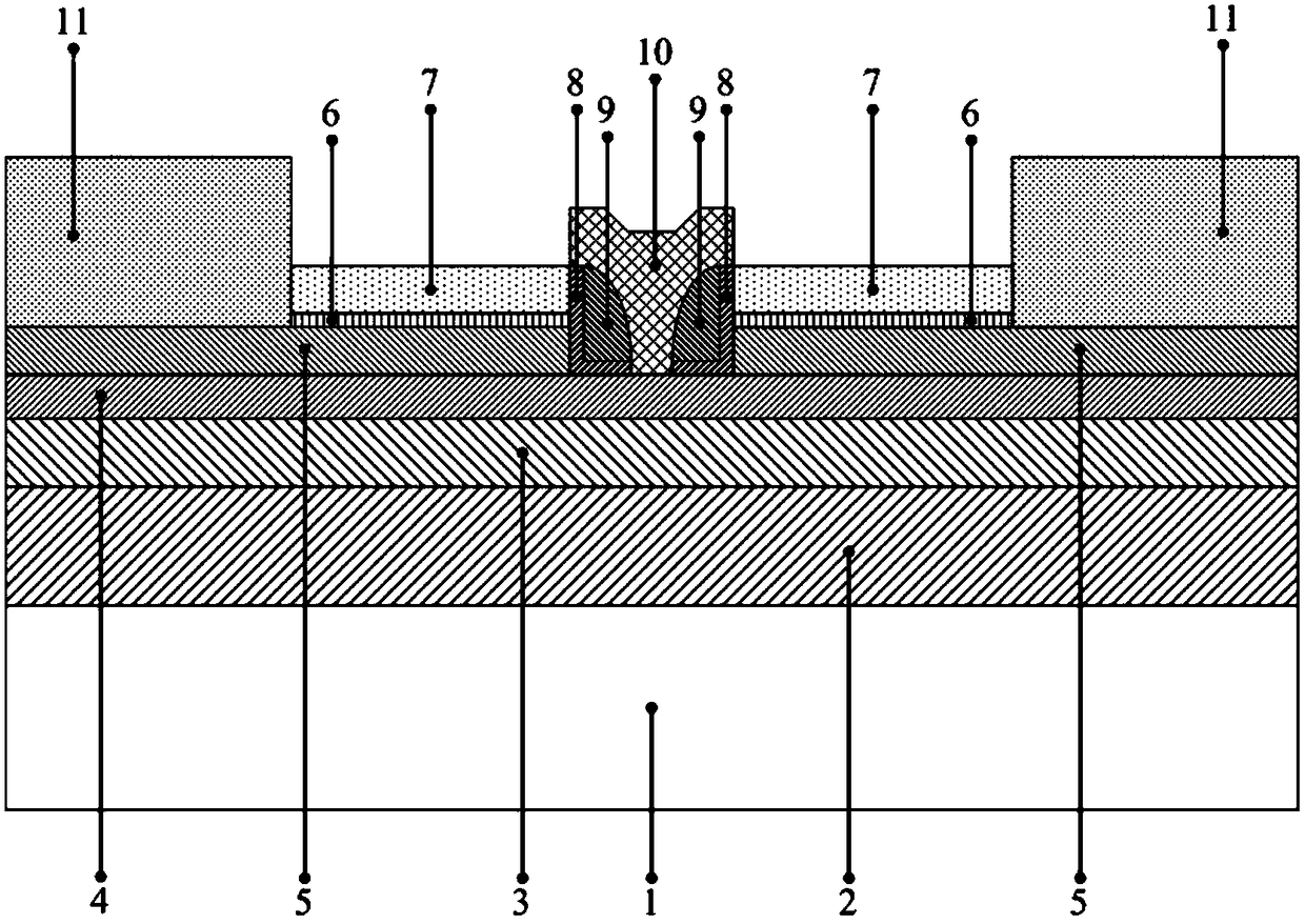
[0040] This embodiment provides a GaN HEMT device. refer to figure 1 As shown, the GaN HEMT device includes a substrate 1, a buffer layer 2, a GaN channel layer 3, a barrier layer 4, an N-type cap layer 5, a first passivation layer 6, a first dielectric layer 7, a second passivation layer layer 8, second dielectric layer 9, gate metal layer 10 and source-drain metal layer 11.

[0041]Wherein, the buffer layer 2 is stacked on the substrate 1; the GaN channel layer 3 is stacked on the buffer layer 2; the barrier layer 4 is stacked on the GaN channel layer 3; the N-type cap layer 5 is stacked on the barrier layer 4; the source-drain metal layer 11 is stacked on the outer edge of the N-type cap layer 5, and the first A passivation layer 6 is also stacked on the N-type cap layer 5, the first dielectric layer 7 is stacked on the first passivation layer 6, the first passivation layer 6 and the The first dielectric layer 7 is located between the source and drain metal layers on bot...

Embodiment 2

[0055] This embodiment provides a method for preparing a GaN HEMT device, including the following steps:

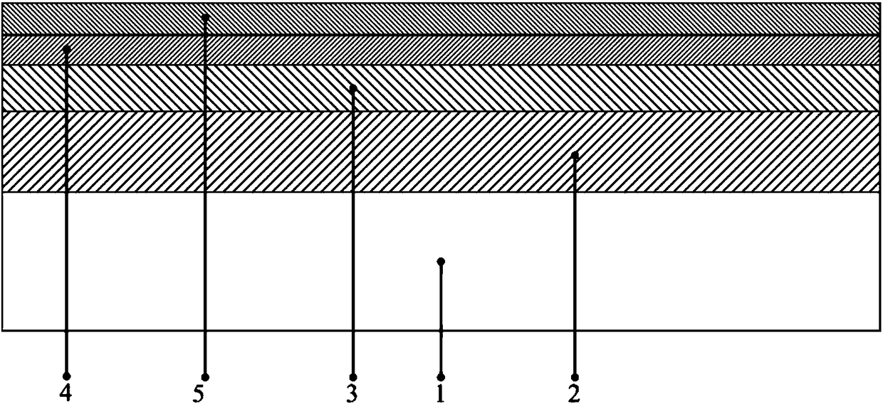
[0056] S1. Epitaxially form buffer layer 2, channel layer 3, barrier layer 4 and N-type cap layer 5 sequentially on substrate 1, such as figure 2 shown;

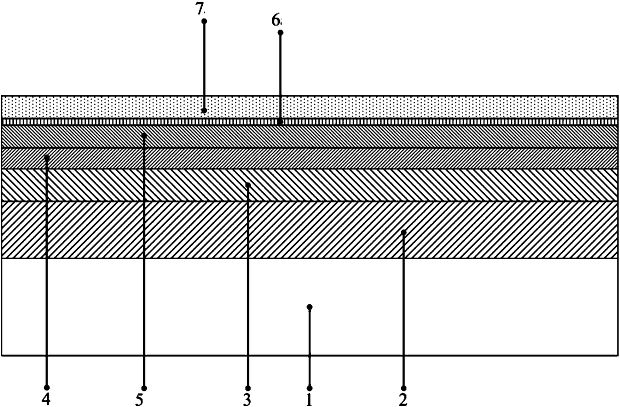
[0057] S2. Deposit the first passivation layer 6 and the first dielectric layer 7 sequentially on the N-type cap layer 5, and selectively remove part of the first passivation layer, part of the first dielectric layer and part of the N-type by dry etching cap layer, thereby forming a gate metal region 12 penetrating through the middle of the first dielectric layer 7, the first passivation layer 6 and the N-type cap layer 5, such as image 3 and 4 shown;

[0058] S3, sequentially depositing the second passivation layer 8 and the second dielectric layer 9, dry etching the second passivation layer 8 and the second dielectric layer 9 to make the upper surface of the barrier layer 4 located in the gate metal region 12 Th...


PUM

PropertyMeasurementUnit
widthaaaaaaaaaa
widthaaaaaaaaaa
thicknessaaaaaaaaaa

Abstract

The invention discloses a GaN (Gallium Nitride) HEMT (High Electron Mobility Transistor) device and a preparation method thereof. The GaN HEMT device comprises an N-type cap layer, a first passivationlayer and a first dielectric layer, wherein a gate metal region is penetrated in the middle parts of the N-type cap layer, the first passivation layer and the first dielectric layer; a second passivation layer is formed in the gate metal region and covers the lateral surfaces of the N-type cap layer, the first passivation layer and the first dielectric layer exposed in the gate metal region and apart of the upper surface of a barrier layer; a second dielectric layer is formed in the gate metal region and is superposed on the second passivation layer; a gate metal layer covers the residual upper surface of the barrier layer exposed in the gate metal region, the second passivation layer and the second dielectric layer; and the second passivation layer and the second dielectric layer are superposed at two sides of the gate metal layer. The N-type cap layer is adopted to reduce the parasitic resistance of a source and a drain, and a lateral wall process is adopted to manufacture the second passivation layer and the second dielectric layer which are superposed at two sides of the gate metal layer to reduce the gate length size and reduce the parasitic capacitance, thereby obtaining the GaN HEMT device with excellent radio frequency characteristics.

Description

technical field [0001] The invention belongs to the field of semiconductor devices, and in particular relates to a GaN HEMT device and a preparation method thereof. Background technique [0002] The research and application of GaN materials and devices is the frontier and hotspot of global semiconductor research. Together with SiC and diamond materials, GaN materials are known as the third-generation semiconductor materials. GaN material has the advantages of wide band gap, high critical breakdown electric field, high electron saturation velocity, high thermal conductivity, and high concentration of two-dimensional electron gas at the heterojunction interface. It is an ideal substitute for next-generation power and radio frequency devices. [0003] Traditional GaN HEMT devices adopt a non-doped barrier layer structure, resulting in relatively large source-drain parasitic resistance, which severely limits the high-frequency characteristics of GaN HEMT devices. In order to im...

Claims


Application Information

Patent Timeline
Patent Type & Authority Applications(China)
IPC IPC(8): H01L29/778H01L29/423H01L21/335
CPCH01L29/42376H01L29/66462H01L29/7786
Inventor 刘洪刚孙兵常虎东
Owner WAYTHON INTELLIGENT TECH SUZHOU CO LTD
Why Eureka
Try Eureka