

Preparation method of palladium diselenide two-dimensional crystalline state film layer
A thin-film layer and crystalline technology, which is applied in the field of preparation of double-layer thin-film structures, can solve the problems of low efficiency and large-scale adoption, and the lack of preparation of two-dimensional crystalline palladium diselenide thin films.
- Summary
- Abstract
- Description
- Claims
- Application Information
AI Technical Summary
Problems solved by technology
Method used
Image

Examples
Embodiment Construction
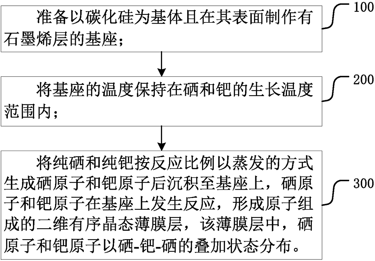
[0022] Such as figure 1 Shown, the preparation method of the palladium diselenide two-dimensional crystalline film layer of an embodiment of the present invention generally comprises the steps:
[0023] Step 100, preparing a base with silicon carbide as the substrate and a graphene layer on its surface;
[0024] The base here is obtained after processing the 6H-silicon carbide substrate in a vacuum environment; in addition to the specified graphene layer that needs to be obtained, it is also necessary to perform a flattening operation on the generated graphene layer. The specific processing process includes: first The 6H-silicon carbide is heated and degassed at 600°C, and then heated repeatedly at 1250-1300°C until a flat graphene layer is formed on the surface of the 6H-silicon carbide.
[0025] Step 200, keeping the temperature of the base within the growth temperature range of selenium and palladium;
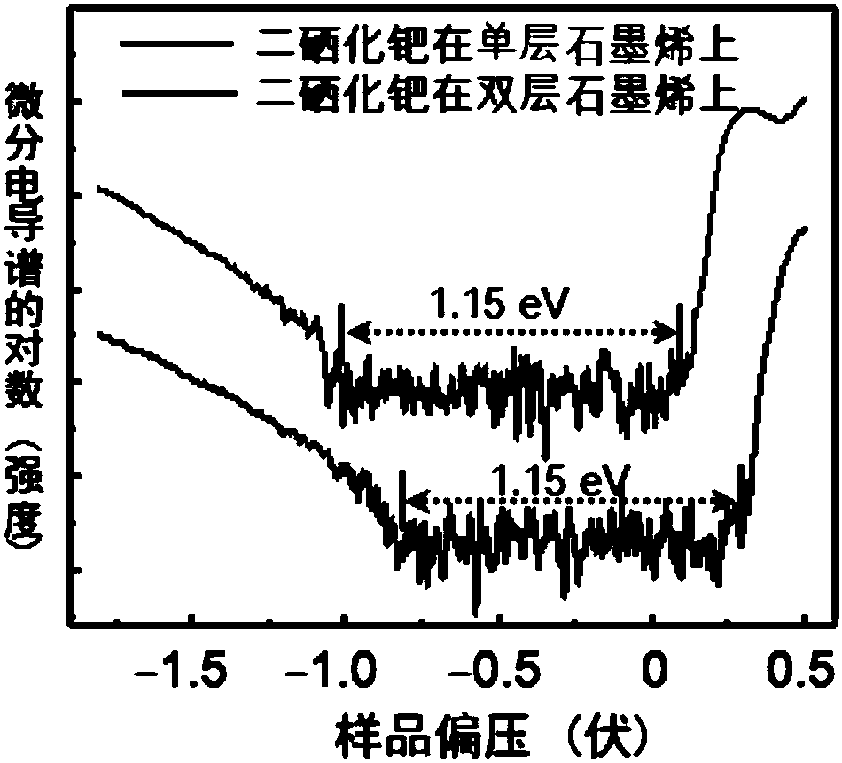
[0026] It is found through experiments that selenium and palladium ca...
PUM
 Abstract
Description
Claims
Application Information