Supercharge Your Innovation With Domain-Expert AI Agents!

Lateral transistor and manufacturing method thereof

A technology of lateral transistors and manufacturing methods, which is applied in semiconductor/solid-state device manufacturing, semiconductor devices, electrical components, etc., and can solve the problems of low device emitter emissivity and poor current amplification capability

Inactive Publication Date: 2018-09-07
汇佳网(天津)科技有限公司
View PDF9 Cites 0 Cited by
  • Summary
  • Abstract
  • Description
  • Claims
  • Application Information

AI Technical Summary

Problems solved by technology

[0004] In view of this, the object of the present invention is to provide a lateral transistor and its manufacturing method, so as to alleviate the technical problems of low device emitter emittance and poor current amplification capability in the prior art

Method used


Image

  • Lateral transistor and manufacturing method thereof
  • Lateral transistor and manufacturing method thereof
  • Lateral transistor and manufacturing method thereof

Examples


Embodiment 1

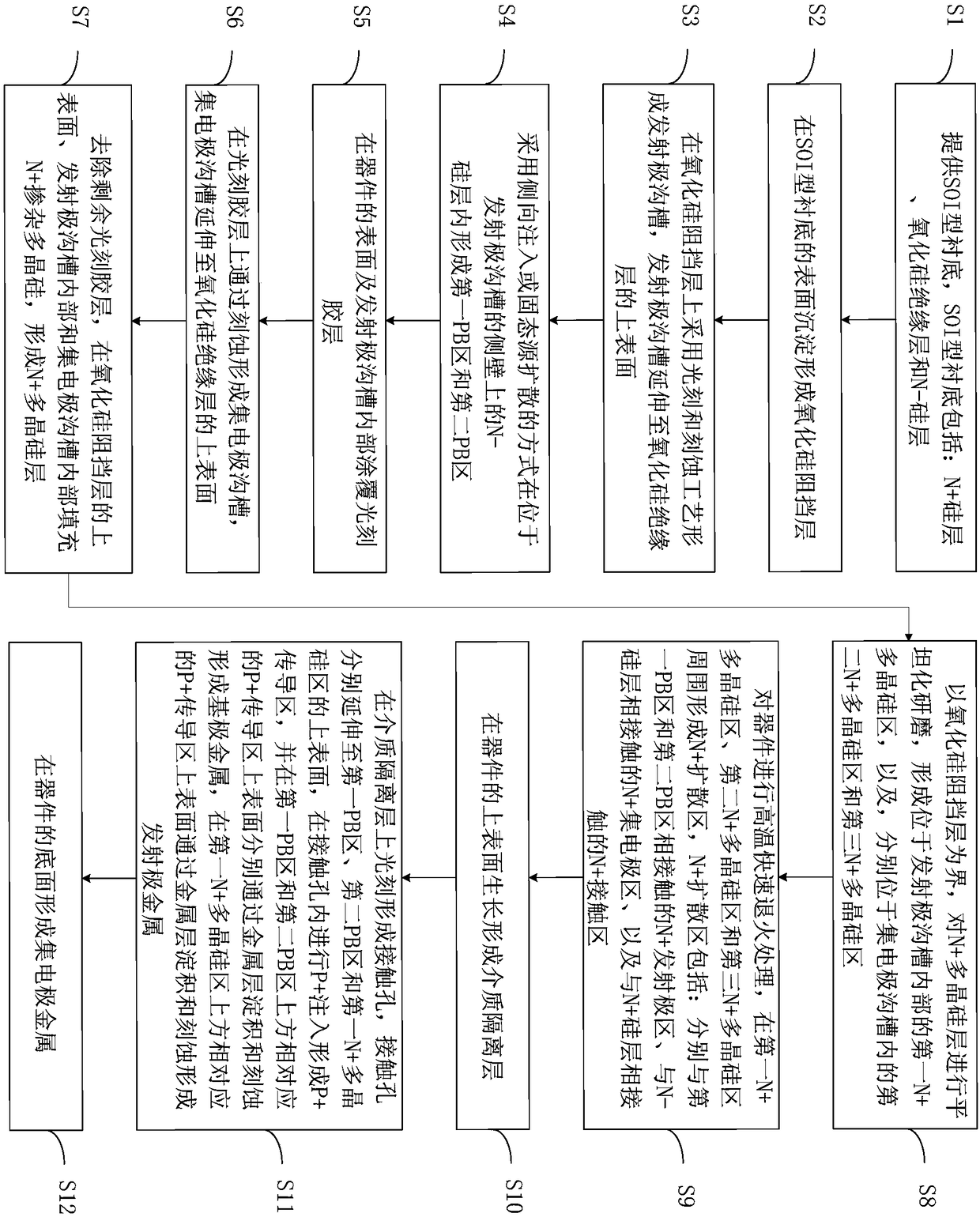
[0051] see figure 1 , a flowchart of a method for fabricating a lateral transistor provided by an embodiment of the present invention. A method for fabricating a lateral transistor provided in an embodiment of the present invention includes the following steps:

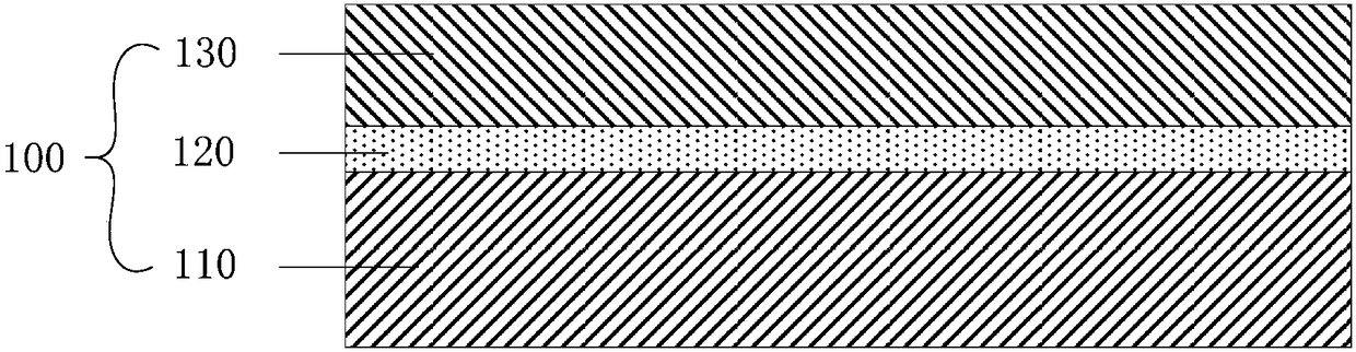
[0052] Step 1: Provide an SOI type substrate 100 , which sequentially includes an N+ silicon layer 110 , a silicon oxide insulating layer 120 and an N − silicon layer 130 from bottom to top. see figure 2 , a product schematic diagram of Step 1 in the method for fabricating a lateral transistor provided in an embodiment of the present invention.

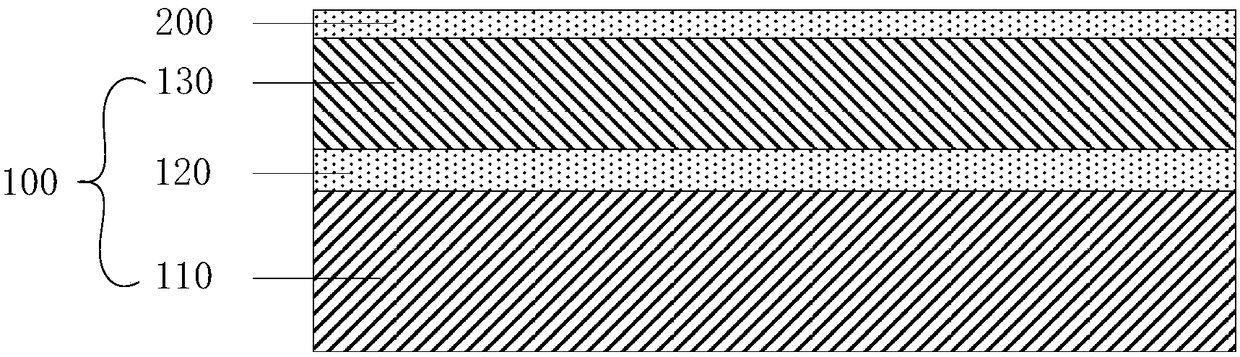
[0053] Step 2: forming a silicon oxide barrier layer 200 by depositing on the surface of the SOI substrate. see image 3 , a product schematic diagram of Step 2 in the method for fabricating a lateral transistor provided in an embodiment of the present invention.

[0054] Step 3: Form an emitter trench on the silicon oxide blocking layer 200 by photolithography and etch...

Embodiment 2

[0067] A lateral transistor provided by an embodiment of the present invention is prepared according to the above method for manufacturing a lateral transistor, including: an SOI substrate, a silicon oxide barrier layer, a first PB region, a second PB region, and a first N+ polysilicon region, the second N+ polysilicon region, the third N+ polysilicon region, N+ diffusion region, dielectric isolation layer, P+ conduction region, emitter metal, base metal and collector metal. Wherein, the SOI type substrate includes: N+ silicon layer, silicon oxide insulating layer and N- silicon layer, and the N+ diffusion area includes: N+ emitter area, N+ collector area and N+ contact area. see Figure 13 , in the manufacturing method of the lateral transistor provided in the above embodiment, the product in the product schematic diagram in step 12 is the structural schematic diagram of the lateral transistor provided in the embodiment of the present invention.

[0068] The silicon oxide ba...


PUM

PropertyMeasurementUnit
Widthaaaaaaaaaa
Widthaaaaaaaaaa

Abstract

The invention provides a lateral transistor and a manufacturing method thereof and relates to the technical field of semiconductor chips. Firstly, an SOI type substrate is provided to form a silicon oxide barrier layer and form a first PB region and a second PB region; secondly, a photoresist layer is coated, a collector trench is formed on the photoresist layer, the remaining photoresist layer isremoved to form a first N+ polysilicon region, a second N+ polysilicon region, and a third N+ polysilicon region; and then, high temperature rapid annealing processing is carried out on the device toform an N+ diffusion region; finally, a dielectric isolation layer and a P+ conduction region are formed, and base metal, emitter metal, and collector metal are formed. The technical scheme realizesthe uniform distribution of the PN junction doping concentration in the device, improves the emission efficiency of the emitter, improves the current capability of the device, as well as reduces the difficulty of the device fabrication process, ensures the stability of the device quality, and further alleviates the technical problem that the emitter of the device has low emissivity and poor current amplification capability in the prior art.

Description

technical field [0001] The invention relates to the technical field of semiconductor chips, in particular to a lateral transistor and a manufacturing method thereof. Background technique [0002] Crystal triode is one of the basic components of semiconductors. It has the function of current amplification and is the core component of electronic circuits. The triode is made on a semiconductor substrate with two PN junctions that are very close to each other. The two PN junctions divide the positive semiconductor into three parts. The middle part is the base area, and the two sides are the emitter area and the collector area. The arrangement is PNP. Compared with NPN, NPN tubes have stronger current amplification capabilities and are more widely used in practical applications. In a typical integrated vertical NPN transistor structure, BN is the collector buried layer, DN is the collector phosphorus bridge, and the BN-DN circuit can reduce the collector resistance and increase ...

Claims


Application Information

Patent Timeline
IPC IPC(8): H01L21/331H01L29/08H01L29/10H01L29/735
CPCH01L29/0808H01L29/0821H01L29/1008H01L29/6625H01L29/735
Inventor 刘自奇
Owner 汇佳网(天津)科技有限公司
Features
  • R&D
  • Intellectual Property
  • Life Sciences
  • Materials
  • Tech Scout
  • Unparalleled Data Quality
  • Higher Quality Content
  • 60% Fewer Hallucinations
Learn More