
Substrate integration waveguide wide-band filter with high selectivity

A substrate-integrated waveguide, high-selectivity technology, applied to waveguide devices, electrical components, circuits, etc., can solve the problems of increasing filter volume, selectivity, noise figure gain and sensitivity, and increasing filter loss. , to achieve low insertion loss, improved frequency selection characteristics, and high Q value

Inactive Publication Date: 2018-09-07
XIDIAN UNIV
View PDF2 Cites 1 Cited by
  • Summary
  • Abstract
  • Description
  • Claims
  • Application Information

AI Technical Summary

Problems solved by technology

However, with the increase in the number of resonant cavities, not only the size of the filter is increased, but also the loss of the filter is increased, which directly affects the selectivity, noise figure, gain and sensitivity of the communication system.

Method used


Image

  • Substrate integration waveguide wide-band filter with high selectivity
  • Substrate integration waveguide wide-band filter with high selectivity
  • Substrate integration waveguide wide-band filter with high selectivity

Examples


Embodiment Construction

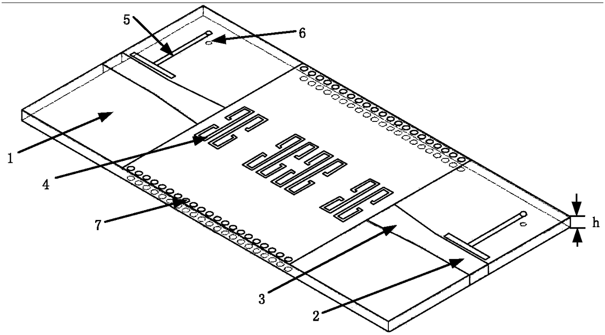
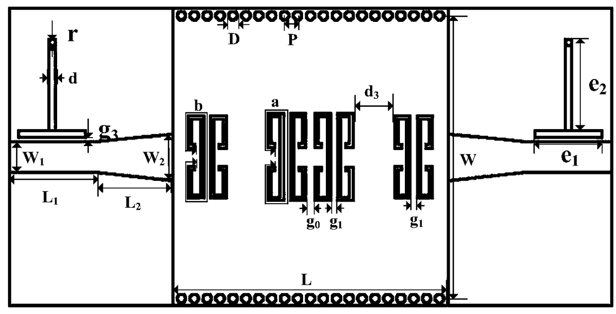
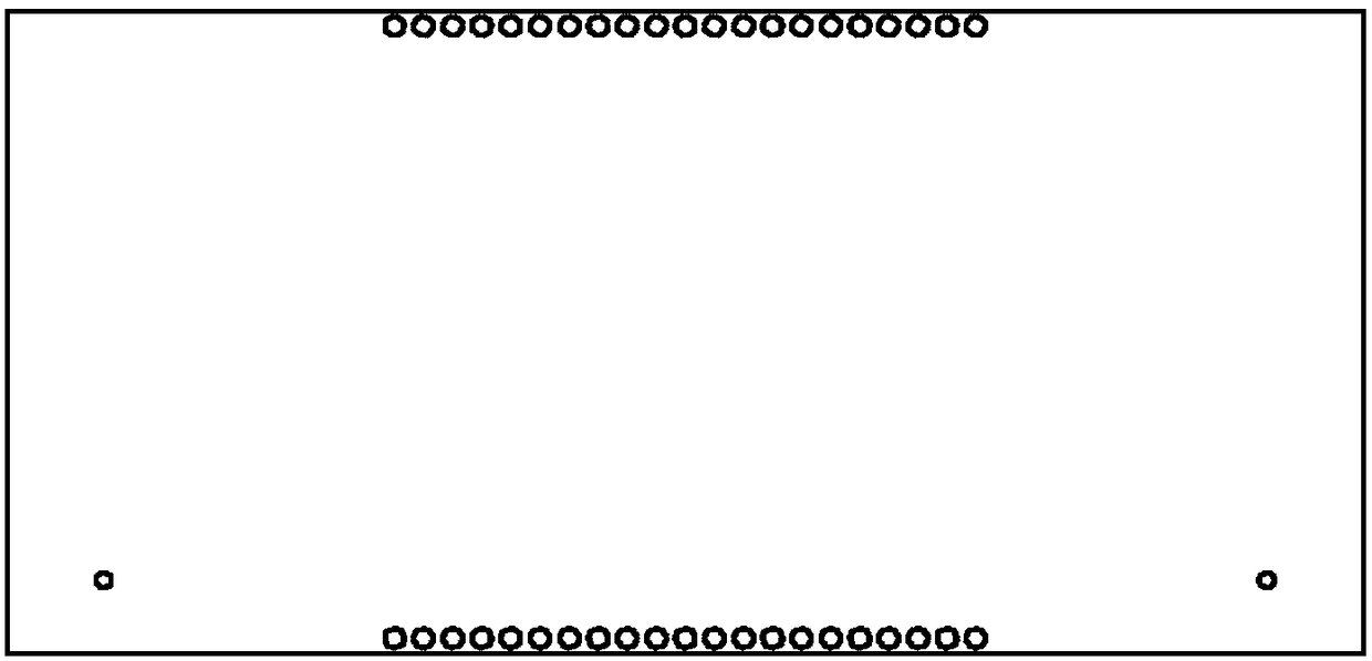
[0018] refer to figure 1 , figure 2 with image 3 , the present invention includes a substrate integrated waveguide 1, a 50Ω microstrip transmission line 2, a trapezoidal progressive microstrip transmission line 3, a meander defect ground structure 4 and a ground stub loaded resonator 5. in:

[0019] The upper and lower bottom surfaces of the substrate integrated waveguide 1 are metal layers, and the middle is a low-loss dielectric substrate with a dielectric constant of ε=2.2. In this example, Rogers RT / duroid 5880 is used, and its thickness is h=0.508mm. It is two rows of metallized through holes 7, the distance between the centers of the two rows of metal through holes 7 is 16 mm to 17 mm, and the distance P between adjacent metal through holes is a value less than a quarter of the wavelength of the waveguide, and satisfies P<4D, D is the diameter of the through hole 7, but not limited to P=1.5mm, D=1mm, W=16.5mm, L=16mm in this example.

[0020] The 50Ω microstrip tra...


PUM


Abstract

The present invention discloses a substrate integration waveguide wide-band filter with high selectivity by employing a defected ground plane and a grounding branchknot loading resonator. The objective of the invention is to mainly solve the problems that it is difficult to meet miniaturization, low loss and good out-of-band performances at the same time in the prior art. The substrate integrationwaveguide wide-band filter comprises a substrate integration waveguide cavity (1), a 50[Omega] microstrip transmission line (2) and a trapezoidal progressive micro-band transmission line (3) which isin transition connection with the substrate integration waveguide cavity (1) and in smooth connection with the 50[Omega] microstrip transmission line (2); four pairs of symmetrical and non-repetitivezigzag defected ground planes are etched at the center of the upper surface of the substrate integration waveguide cavity (1); and one side of the 50[Omega] microstrip transmission line (2) is next to the grounding branchknot loading resonator (5). The substrate integration waveguide wide-band filter has advantages of high-frequency selectivity, a high Q value, high power capacity, low radiation,low loss, miniaturization and easy connection, and can be applied to the front end of a radio frequency transmitter-receiver set.

Description

technical field [0001] The invention belongs to the technical field of microwave communication devices, in particular to a substrate integrated waveguide broadband filter, which can be used in the design of microwave and millimeter wave circuits. Background technique [0002] As an important component in the field of wireless communication, the bandpass filter's performance is directly related to the performance of the entire system. Traditional bandpass filters are generally divided into planar microstrip or stripline structure filters and metal waveguide structure filters. Although planar microstrip or stripline structure filters are easy to integrate, they have large radiation loss and low Q value. Although the metal waveguide structure filter has the characteristics of low loss, high Q value, and good selectivity, it is bulky and complicated to process and debug, which is not conducive to integration with active circuit substrates. The bandpass filter based on the subs...

Claims


Application Information

Patent Timeline
Patent Type & Authority Applications(China)
IPC IPC(8): H01P1/203H01P1/20
CPCH01P1/203H01P1/20
Inventor 安翔程祥远
Owner XIDIAN UNIV
Learn More