Visible-near-infrared region wide-band perfect absorber and preparation method thereof

A wide-band, absorber technology, applied in the field of visible-near-infrared wide-band perfect absorber and its preparation, can solve problems such as complex structure, narrow wavelength range, strong ohmic loss and thermal effect, and achieve wide application prospects and low cost cheap effect

Inactive Publication Date: 2018-09-11
JIANGXI NORMAL UNIVERSITY
View PDF5 Cites 25 Cited by
  • Summary
  • Abstract
  • Description
  • Claims
  • Application Information

AI Technical Summary

Problems solved by technology

However, in these perfect absorber systems, only electromagnetic waves of a single resonance wavelength can be absorbed, which is a narrow-band light absorption
In addition, these electromagnetic wave perfect absorber systems are all based on noble metal materials (such as gold and silver). The coupling of electromagnetic waves is realized through the free electron oscillation modes of these metal materials. These free electron oscillations will inevitably lead to strong ohmic losses and thermal effects, whic

Method used


Image

  • Visible-near-infrared region wide-band perfect absorber and preparation method thereof
  • Visible-near-infrared region wide-band perfect absorber and preparation method thereof
  • Visible-near-infrared region wide-band perfect absorber and preparation method thereof

Examples


Embodiment Construction

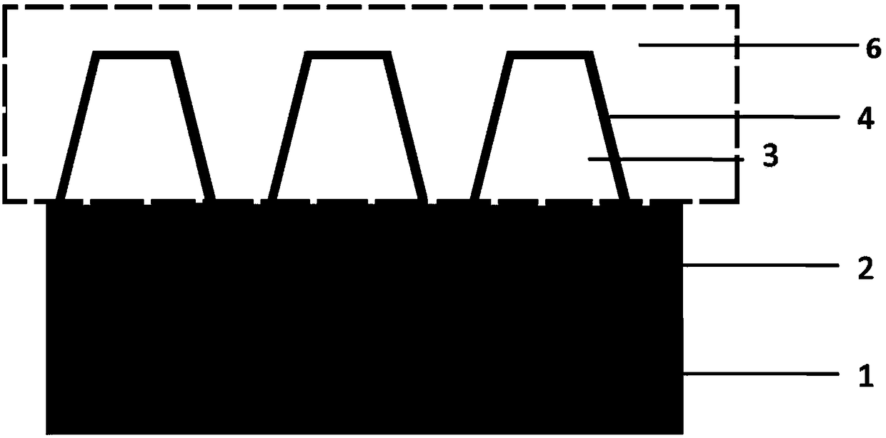
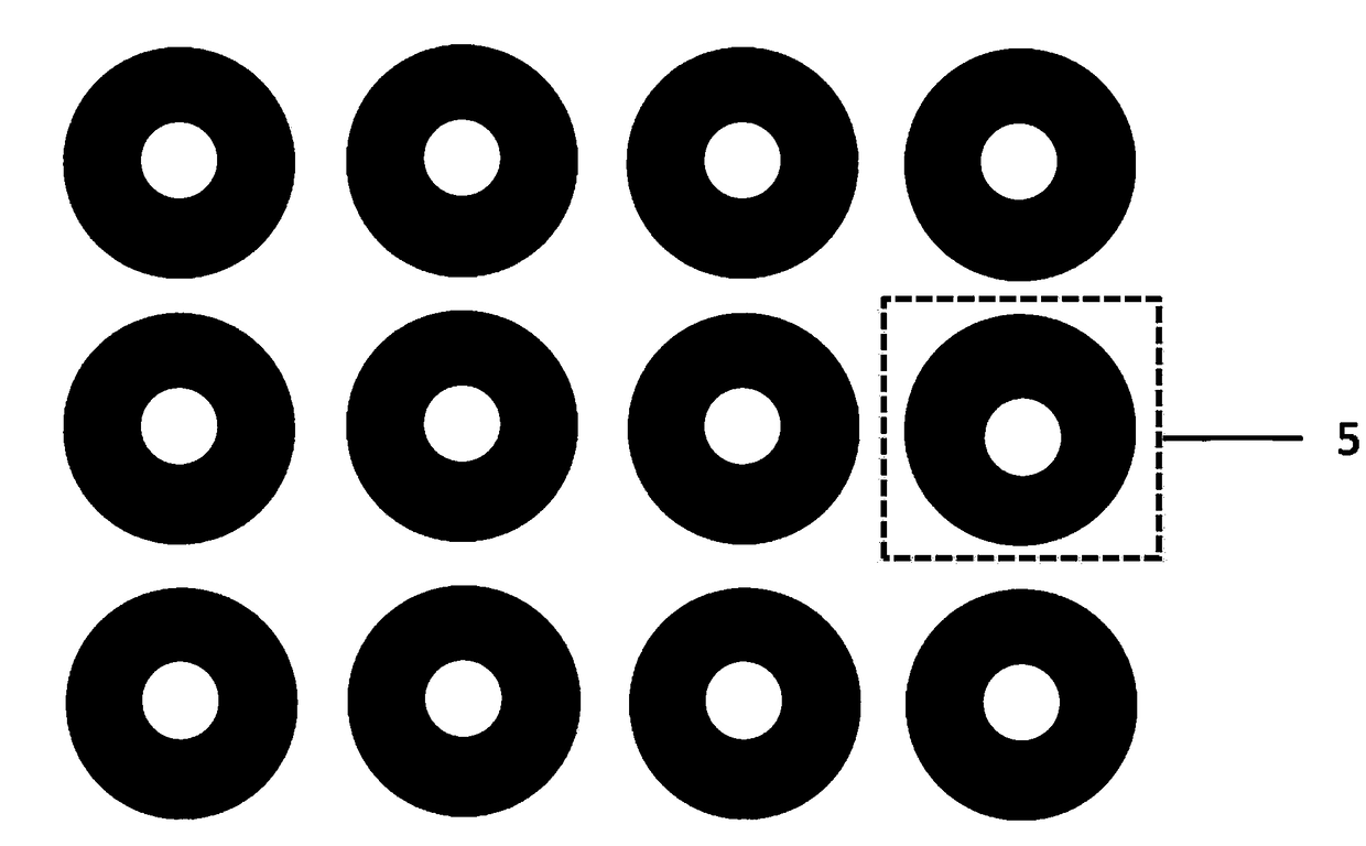
[0032] Attached below Figure 1-6 The present invention is described in detail, but the following drawings are only schematic diagrams of idealized embodiments of the present invention, wherein in order to clearly show the structure of the device involved in the present invention, the selected metal-medium conical column particle structure wherein The thickness of the layer region is appropriately exaggerated, but as a schematic, it should not be considered to strictly reflect the proportional relationship of the geometric dimensions. In addition, the illustrated embodiments of the invention should not be construed as limited to the specific shapes of regions illustrated in the drawings. In general, the following figures are schematic and should not be considered as limiting the scope of the invention.

[0033] A wide-band perfect absorber in the visible-near-infrared region, including a substrate 1, a metal film layer 2, and a metal-medium conical cylinder composite structur...


PUM

PropertyMeasurementUnit
Thicknessaaaaaaaaaa
Diameteraaaaaaaaaa
Diameteraaaaaaaaaa

Abstract

The invention relates to a visible-near-infrared region wide-band perfect absorber. The visible-near-infrared region wide-band perfect absorber includes a substrate, a metal film layer and a metal-dielectric conical cylindrical composite structural layer; the metal-dielectric conical cylindrical composite structural layer is arranged on the metal film layer; and the metal film layer is arranged onthe substrate. With the visible-near-infrared region wide-band perfect absorber of the invention adopted, problems such as internal metal ohmic loss, thermal effect and thermal instability can be effectively avoided; the wide-band absorption of visible-near-infrared bands can be realized; and plasmon resonance modes within in a plurality of frequency ranges are generated, so that a wide-band electromagnetic wave perfect absorption characteristic can be obtained. The visible-near-infrared region wide-band perfect absorber of the invention has a wide application prospect in the fields of photoelectric devices such as infrared detection and photoelectric conversion devices, infrared imaging devices, solar anti-reflection coatings and heat radiators under high-temperature and high-heat conditions.

Description

technical field [0001] The invention relates to the fields of photoelectric functional materials and devices, solar photovoltaics and thermal radiation, and in particular to a wide-band perfect absorber in the visible-near-infrared region and a preparation method thereof. Background technique [0002] Surface plasmon resonance (SPR) usually refers to the collective oscillation caused by free electrons on the surface of metal microstructures under the irradiation of electromagnetic waves, forming a local electromagnetic field enhancement effect on the metal surface. [0003] Metamaterials refer to artificially designed and manufactured composite materials with periodic structural properties. In recent years, their research has rapidly become a frontier interdisciplinary field of physics, functional technology and material science. [0004] The concept of a perfect absorber was first proposed in 2008 ("Physical Review Letters", Vol. 100, p. 207402), which is a device based on ...

Claims


Application Information

Patent Timeline
IPC IPC(8): H01L31/0352H01L31/04H01L31/09H01L31/18
CPCH01L31/0352H01L31/04H01L31/095H01L31/18H01L31/186Y02E10/50Y02P70/50
Inventor 刘正奇唐鹏李玉银刘桂强
Owner JIANGXI NORMAL UNIVERSITY
Why Eureka
Try Eureka