
Low prevention zone difference transmission structure employing silicon through hole and interlayer interconnection structure

A technology of differential transmission and through-silicon vias, which is applied in the direction of electrical components, electrical solid-state devices, circuits, etc., can solve the problems of unfavorable three-dimensional integrated circuit transistors closely arranged and the increase of the blocking area, so as to reduce the blocking layout layer and integrate The effect of improving the speed and isolating external interference

Inactive Publication Date: 2018-09-14
HANGZHOU DIANZI UNIV
View PDF5 Cites 11 Cited by
  • Summary
  • Abstract
  • Description
  • Claims
  • Application Information

AI Technical Summary

Problems solved by technology

In this regard, some people have proposed a differential TSV transmission structure with a ground-signal-signal-ground structure to ensure the transmission quality of high-speed signals, but this structure cannot avoid crosstalk between differential pairs
Later, someone proposed a shielded differential through-silicon via structure (CN 105810663 A), which can effectively shield the crosstalk between differential pairs and further improve the quality of signal transmission. However, due to its large diameter shielding structure and thermal stress during processing Existence, the blocking area is also significantly increased, which is not conducive to the tight arrangement of three-dimensional integrated circuit transistors

Method used


Image

  • Low prevention zone difference transmission structure employing silicon through hole and interlayer interconnection structure
  • Low prevention zone difference transmission structure employing silicon through hole and interlayer interconnection structure
  • Low prevention zone difference transmission structure employing silicon through hole and interlayer interconnection structure

Examples


Embodiment Construction

[0027] The present invention will be further described below in conjunction with accompanying drawing.

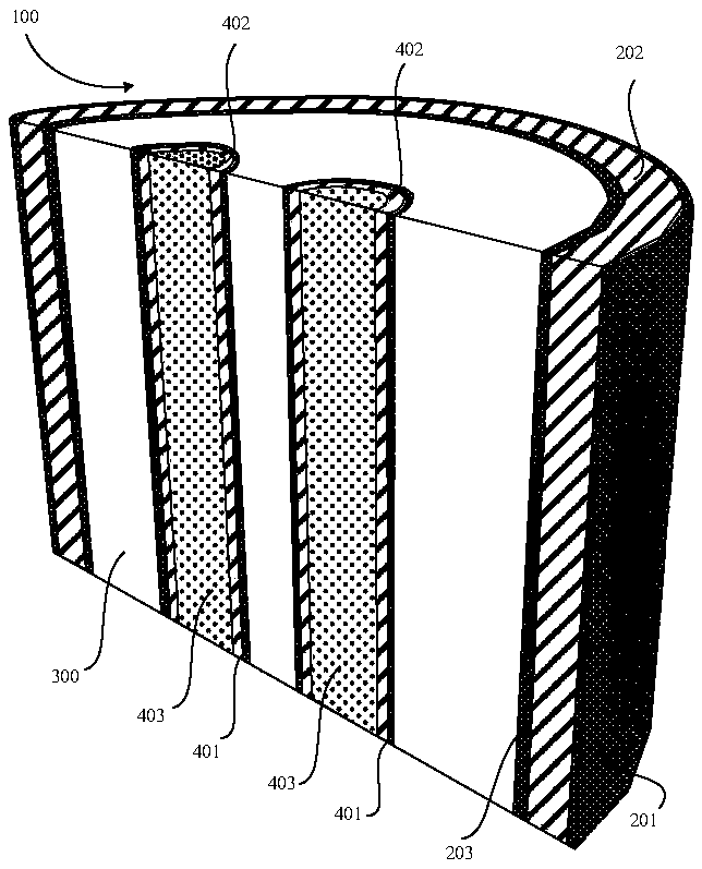
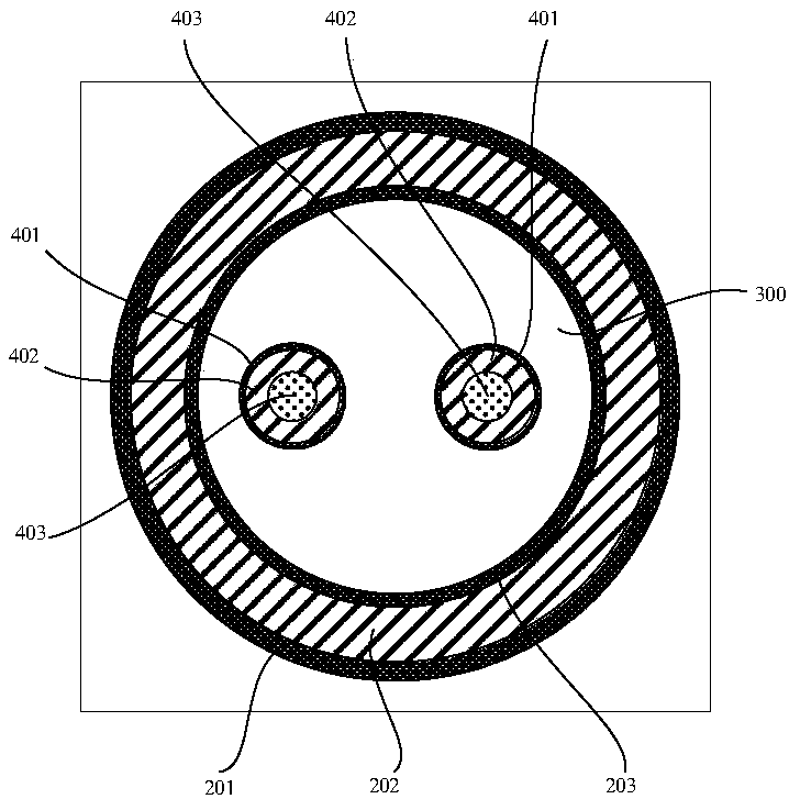
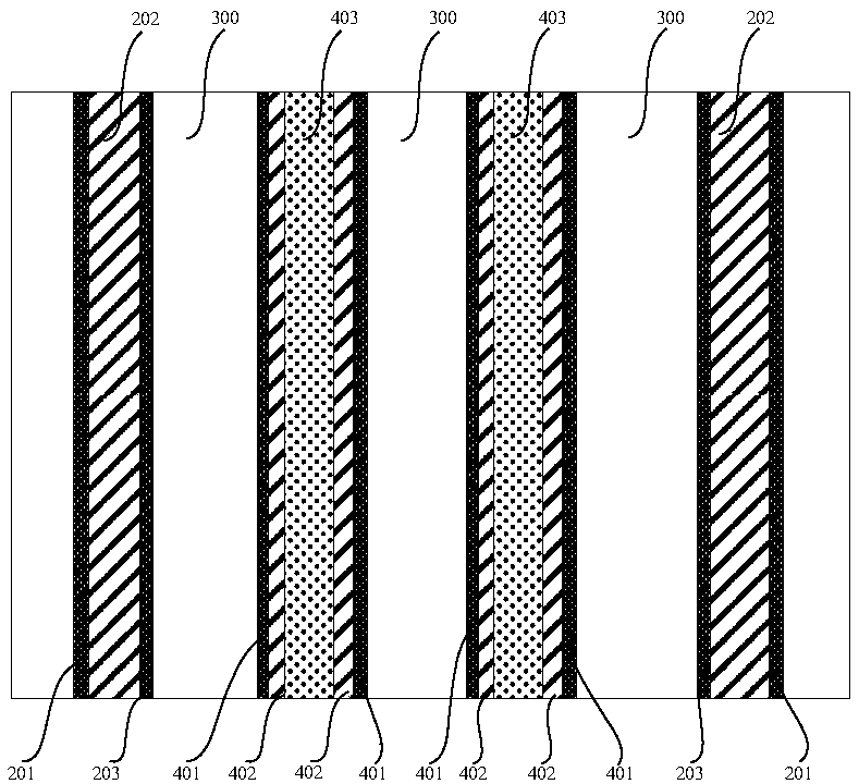
[0028] Such as figure 1 , 2 , 3, the differential transmission structure 100 using annular TSVs is located in the silicon substrate, and includes an outer shielded TSV 200 , an inner silicon substrate 300 and an inner differential TSV 400 from outside to inside.

[0029] Such as Figure 4 As shown, the external shielding TSV 200 is not only a current return path of the differential transmission line, but also a shielding shell of the differential transmission line (for isolating external interference). The shielded TSV 200 is composed of a first dielectric layer 201 , an outer annular TSV inner core 202 and a second dielectric layer 203 . The first dielectric layer 201 is used to isolate and shield DC leakage between the TSV and the silicon substrate, and is composed of insulating materials such as silicon dioxide or silicon nitride. The outer annular TSV core 202 is fi...


PUM


Abstract

The invention discloses a low prevention zone difference transmission structure employing a silicon through hole and an interlayer interconnection structure. In the low prevention zone difference transmission structure and the interlayer interconnection structure, excellent electric transmission performance of the difference silicon through hole is shielded while thermodynamics characteristics ofa difference silicon through hole transmission structure are improved. Reduction of a prevention layout zone can be caused by mismatching thermal stress when the difference transmission structure employing the silicon through hole, and integrated level improvement of transistors in a large scale array can be facilitated. In actual application of a three dimensional integrated circuit, the low prevention zone difference transmission structure and the interlayer interconnection structure normally relate to difference signal transmission between multilayer structures. Aimed at improving transmission efficiency, the invention discloses a cross-connect method for interlayer structures.

Description

technical field [0001] The invention belongs to the field of three-dimensional integrated circuits, and in particular relates to a high-performance differential transmission structure using annular through-silicon holes and an interlayer interconnection structure. Background technique [0002] As one of the key technologies of 3D integrated circuits, through-silicon via technology has been extensively studied. Using through-silicon via technology, three-dimensional integrated circuits can achieve higher integration, shorter interconnection lengths, better noise suppression capabilities, and lower capacity loss. However, with the increase of signal frequency, the signal integrity problems brought by TSV technology are also becoming more and more obvious, mainly reflected in the crosstalk between TSVs and the current leakage between TSVs and the substrate. On the other hand, in the actual processing process, due to the differences in the thermal expansion coefficients of vari...

Claims


Application Information

Patent Timeline
IPC IPC(8): H01L23/528H01L23/532H01L23/552H01L21/768
CPCH01L23/5283H01L21/76802H01L21/76819H01L23/53228H01L23/53276H01L23/552
Inventor 赵文生傅楷徐魁文董林玺王高峰
Owner HANGZHOU DIANZI UNIV
Learn More