Three-dimensional stacked interconnection structure for SiC device based on nano-silver soldering paste, and preparation method

An interconnect structure, three-dimensional stacking technology, applied in semiconductor/solid-state device manufacturing, nanotechnology for materials and surface science, nanotechnology, etc. Parasitic inductance and resistance, etc., to alleviate the edge breakdown effect, shorten the interconnection distance, and increase the contact area.

Active Publication Date: 2018-09-18
INST OF ELECTRONICS ENG CHINA ACAD OF ENG PHYSICS
View PDF8 Cites 6 Cited by
  • Summary
  • Abstract
  • Description
  • Claims
  • Application Information

AI Technical Summary

Problems solved by technology

[0002] Silicon carbide is a typical third-generation semiconductor material. With the continuous development of the electronics industry, silicon carbide devices have emerged as the times require. Its operating temperature is high and its withstand voltage is high. It is difficult for the old packaging form to fully utilize the advantages of silicon carbide devices.
The demand for packaging of silicon carbide devices is mainly reflected in high-temperature and high-pressure packaging. At present, there are few research institutes for silicon carbide device packaging. The packaging of multi-silicon carbide power chips is mostly in the form of modules, which are bulky and can be mounted by solder welding. , wire bonding is used to realize the interconnection of chip electrodes and external terminals. The main problem of solder welding is that the properties of the welding layer material remain unchanged after welding, and its temperature resistance is low, which affects the selection of secondary welding materials. The problem of wire bonding Because the size of the package is limited by the height of the leads, the leads increase the parasitic inductance and resistance, reducing the reliability of the package
Vertical stacking is one of the effective ways to achieve miniaturization and integration. The key factor limiting the development of vertical stacking packaging technology is the interconnection technology between chips. At present, the technology and method of interconnection between chips are still immature, so it is necessary to study new Package form to meet the needs of high temperature and high pressure, while reducing package volume and increasing package reliability
[0003] The applicant has proposed an invention titled a silicon carbide device packaging structure and manufacturing method based on a three-layer DBC substrate, the publication number is CN107393882A, and the publication date is November 24, 2017. The packaging structure in this technical solution includes three layers The patterned DBC substrate forms an upper, middle and lower structure, two layers of nano-silver solder paste, vertical silicon carbide power chips and high-temperature-resistant fillers; but in this solution, chip electrodes are only realized through the patterning of the DBC substrate and the connection of nano-silver solder paste No lead out, can not form a three-bit stacked interconnection structure

Method used


Image

  • Three-dimensional stacked interconnection structure for SiC device based on nano-silver soldering paste, and preparation method
  • Three-dimensional stacked interconnection structure for SiC device based on nano-silver soldering paste, and preparation method
  • Three-dimensional stacked interconnection structure for SiC device based on nano-silver soldering paste, and preparation method

Examples


Embodiment Construction

[0025] The technical solutions in the embodiments of the present invention will be clearly and completely described below in conjunction with the accompanying drawings in the embodiments of the present invention. Obviously, the described embodiments are only some of the embodiments of the present invention, not all of them. Based on the embodiments of the present invention, all other embodiments obtained by persons of ordinary skill in the art without making creative efforts belong to the protection scope of the present invention.

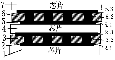
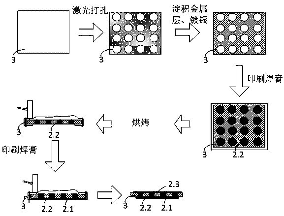
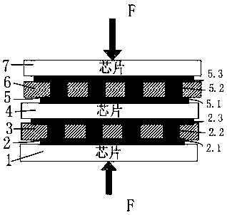
[0026] Embodiments of the present invention provide a three-dimensional stacked structure of SiC devices based on nano-silver solder paste such as figure 1 As shown, it includes: three silicon carbide power chips 1, 4, 7, all of which are vertical structure diodes; two-layer interconnection structures 2, 3, 5, 6. The interconnection structure is composed of ceramic substrates 3 and 6 with through holes and nano-silver solder paste 2 and 5. The diam...


PUM

PropertyMeasurementUnit
pore sizeaaaaaaaaaa

Abstract

The invention provides a three-dimensional stacked interconnection structure for a SiC device based on nano-silver soldering paste, and a preparation method. The interconnection structure comprises the nano-silver soldering paste and a ceramic plate. The nano-silver soldering paste is disposed in through holes in the ceramic plate, and a conductive circuit is formed after sintering. Furthermore, the nano-silver soldering paste is sintered to achieve the stacked interconnection of chip electrodes. The ceramic plate serves as an insulating plate and an underlay layer, thereby increasing the distance between two chips, and avoiding the edge breakdown effect between the chips. The connection of the interconnection structure can achieve the longitudinal interconnection of a plurality of chips,and the selected material comprises a ceramic substrate and a nano-silver soldering paste. The main component of the sinter nano-silver soldering paste is silver, and the conductivity and temperatureresistance of the sintered nano-silver soldering paste are close to the conductivity and temperature resistance of pure silver. The nano-silver soldering paste and the ceramic substrate are both madeof high temperature resistant materials, and can be used for the interconnection of a big power chip. Compared with other parking modes, the structure is simple in structure, is high in operability, is wide in application range, and can achieve the simple and effective high-temperature and high-voltage stacked packaging.

Description

technical field [0001] The present invention relates to the field of packaging of semiconductor power devices, in particular to a three-dimensional stacked interconnection structure and preparation method of SiC devices based on nano-silver solder paste. The nano-silver solder paste is used to fill ceramic through holes and stack interconnections to realize power chips. Three-dimensional stacking. Background technique [0002] Silicon carbide is a typical third-generation semiconductor material. With the continuous development of the electronics industry, silicon carbide devices have emerged as the times require. Its operating temperature is high and its withstand voltage is high. It is difficult for the old packaging form to fully utilize the advantages of silicon carbide devices. The demand for packaging of silicon carbide devices is mainly reflected in high-temperature and high-pressure packaging. At present, there are few research institutes for silicon carbide device pa...

Claims


Application Information

Patent Timeline
Patent Type & Authority Applications(China)
IPC IPC(8): H01L23/538H01L23/373H01L21/04H01L21/768B82Y30/00
CPCB82Y30/00H01L21/0445H01L21/76805H01L21/76879H01L23/3731H01L23/5383H01L23/5384H01L23/5385H01L23/5386
Inventor 杨英坤张龙李俊焘代刚肖承全古云飞银杉张林徐星亮向安周阳李志强崔潆心
Owner INST OF ELECTRONICS ENG CHINA ACAD OF ENG PHYSICS
Why Eureka
Try Eureka