mems galvanometer laser microdisplay
A technology of microdisplay and laser, applied in instruments, optics, optical components, etc., can solve problems such as image pincushion distortion, and achieve the effects of low cost, low energy consumption, and small size
- Summary
- Abstract
- Description
- Claims
- Application Information
AI Technical Summary
Problems solved by technology
Method used
Image
Examples
Embodiment 1
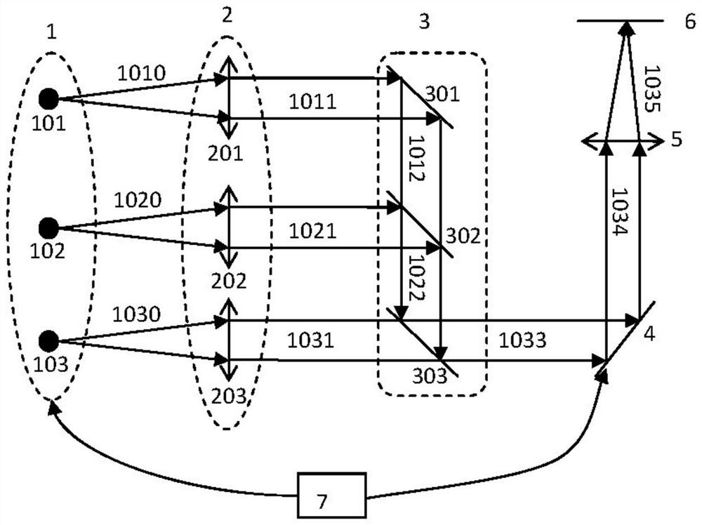
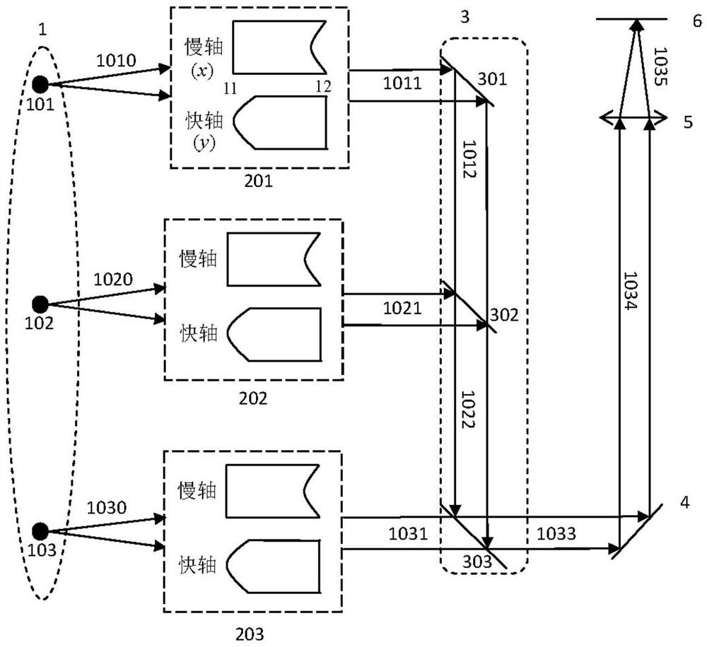
[0130] Example 1: See figure 2 It is a structural schematic diagram of a MEMS galvanometer laser microdisplay in the first embodiment of the present invention. The structure and the structure of the MEMS galvanometer laser microdisplay in this embodiment figure 1 The structures shown are essentially the same. Since the divergence angles of semiconductor lasers in the fast axis and slow axis directions are different, in order to obtain a circular spot with good collimation effect, it is necessary to collimate the light beams in the fast axis and slow axis directions respectively. In this embodiment 1, the collimating and shaping optical system 2 (that is, the laser collimating and shaping optical path) is completed by a single irregular lens, and the single irregular lens is a cylindrical surface whose two front and rear faces are orthogonal, and the curvature is aspherical. The first surface 11 of the single irregular lens adopts a convex structure. In the direction of th...
Embodiment 2
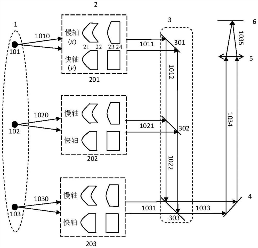
[0131] Example 2: image 3 It is a structural schematic diagram of a MEMS galvanometer laser microdisplay in the second embodiment of the present invention. The structure of the MEMS galvanometer laser microdisplay in this embodiment is basically the same as that of Embodiment 1, the only difference is that the collimation and shaping optical system uses two lenses to realize the collimation and shaping of the laser beam, wherein the first lens is not Regular structure, the second lens is plano-convex structure. In Embodiment 2, the first surface 21 of the first lens adopts a rotating aspheric surface, and the surface 21 realizes the collimation of the fast-axis and slow-axis beams at the same time, so the shape of the beam emitted from the surface 21 is a collimated and parallel elliptical spot . The second surface 22 of the first lens and the first surface 23 of the second lens are all aspheric surfaces in the slow axis direction, and both (face 22 and surface 23) form a G...
Embodiment 3
[0132] Example 3: Figure 4 It is a structural schematic diagram of a MEMS galvanometer laser microdisplay in the third embodiment of the present invention. The structure of the MEMS galvanometer laser microdisplay in this embodiment is basically the same as in Embodiment 2, the only difference is that the collimation and shaping optical system uses three lenses to realize the collimation and shaping of the laser beam, and the three lenses all adopt a plano-convex structure. In Embodiment 3, the first surface 31 of the first lens is the same as the first surface 21 of the first lens in Embodiment 2, that is, the surface 31 can also realize the collimation of the fast-axis and slow-axis light beams at the same time . Both the second surface 34 of the second lens and the first surface 35 of the third lens are aspherical in the direction of the slow axis, and they form a Kepler telescope structure to realize beam expansion in the direction of the slow axis. The remaining faces ...
PUM
| Property | Measurement | Unit |
|---|---|---|
| diameter | aaaaa | aaaaa |
| wavelength | aaaaa | aaaaa |
| divergence angle | aaaaa | aaaaa |
Abstract
Description
Claims
Application Information
 - R&D
- Intellectual Property
- Life Sciences
- Materials
- Tech Scout
- Unparalleled Data Quality
- Higher Quality Content
- 60% Fewer Hallucinations
Browse by: Latest US Patents, China's latest patents, Technical Efficacy Thesaurus, Application Domain, Technology Topic, Popular Technical Reports.
© 2025 PatSnap. All rights reserved.Legal|Privacy policy|Modern Slavery Act Transparency Statement|Sitemap|About US| Contact US: help@patsnap.com


